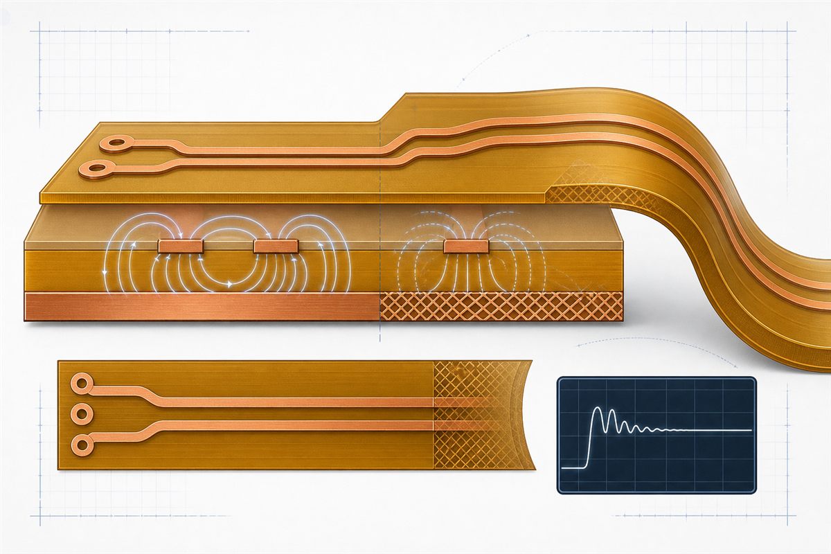
Controlled impedance FPC design begins with the electromagnetic structure, not with a copied line width. Trace geometry, copper thickness, dielectric thickness, material properties, coverlay, reference-plane construction, and the finished fabrication process all influence characteristic impedance. If any of these inputs change, the original calculation may no longer represent the manufactured flex circuit.
What Controlled Impedance FPC Means in Practice
A high-speed trace behaves as a transmission line when its propagation delay becomes significant relative to the signal transition time. Its characteristic impedance is determined by the relationship between the conductor and its return path. The relevant variables include trace width and thickness, dielectric separation, dielectric constant, nearby copper, and—when two traces are coupled—pair spacing and symmetry.
Single-ended impedance describes one signal conductor relative to its return structure. Differential impedance describes the coupled behavior of a pair. Differential impedance is not obtained by simply doubling a single-ended value; coupling between the two conductors and coupling to the reference plane both matter.
Common interfaces may call for nominal single-ended or differential targets, but the interface specification controls the actual requirement. The FPC drawing should state the target, permitted tolerance, impedance type, signal layer, reference layer, and nets or structures to which it applies.
Why FPC Impedance Is Different From Rigid PCB Impedance
A controlled impedance FPC follows the same transmission-line principles as a rigid board, but it introduces a different material system and additional mechanical constraints. Polyimide films are thin, coverlay usually contains both film and adhesive, copper may be rolled annealed or electrodeposited, and the return plane may be crosshatched to improve flexibility. The circuit can also pass through stiffened, bonded, folded, or shielded areas where the local electromagnetic environment changes.
Thin Dielectric Separation
A small trace-to-plane distance can force very narrow traces for a target impedance when a solid adjacent reference plane is used. Manufacturability, etch tolerance, conductor loss, and current requirements must be reviewed together.
Coverlay Construction
The electric field is partly influenced by the coverlay film and adhesive above an outer-layer trace. Treating the structure as bare copper in air can produce an optimistic result.
Mechanical Flexibility
A solid plane improves return-path continuity but increases local copper coverage and bending stiffness. A hatched plane can improve flexibility, but its electromagnetic behavior must be modeled as a mesh rather than as a continuous sheet.
Multiple Local Stack-Ups
A rigid-flex or locally stiffened design may contain several sub-stacks. A trace can meet its target in the free flex region and encounter a discontinuity where adhesive, shielding, a stiffener, or additional copper enters the field.
For the mechanical construction behind these differences, see the FPC stack-up design guide and FPC copper foil guide.
1. Lock the Controlled Impedance FPC Stack-Up Before Freezing Line Width
An online calculator can be useful for an early feasibility estimate, but it cannot know the exact finished construction your supplier will build. The production model needs the actual base-film thickness, adhesive thickness where applicable, copper type and finished copper thickness, coverlay construction, reference-plane geometry, and material properties used by the selected process.
“Two-layer polyimide FPC” is not a stack-up. A controlled document should identify each dielectric and conductive layer in order, including coverlay and bonding layers that influence the impedance structure. For rigid-flex, document the rigid and flex sub-stacks separately.
2. Use Controlled Impedance FPC Material Data Appropriate to the Frequency
Dielectric constant is not a single universal number for “polyimide.” It varies by product, test method, frequency, resin or adhesive content, moisture condition, and the way the electromagnetic field is distributed through the construction. The value used in a field solver should correspond as closely as practical to the selected material and application.
Datasheet values are useful inputs, but they are not automatically the same as the effective dielectric constant seen by a fabricated microstrip or coplanar structure. When the stack includes polyimide film, acrylic or epoxy adhesive, coverlay, air, and solder mask or shielding materials, a single generic Dk can hide meaningful differences.
The correct approach is to keep the material trade name or approved equivalent, construction, data source, and modeling assumptions with the impedance calculation. If material substitution is allowed, the impedance impact should be reviewed rather than treating all flex laminates as interchangeable.
3. Select the Controlled Impedance FPC Transmission-Line Structure Deliberately
| Structure | Typical FPC Use | Key Review Points |
|---|---|---|
| Microstrip | Outer-layer signal referenced to a plane on the opposite side of the dielectric. | Coverlay effect, trace-to-plane distance, copper thickness, and external environment. |
| Differential microstrip | High-speed pairs routed over a solid or modeled reference plane. | Pair width, edge-to-edge spacing, plane coupling, skew, and routing symmetry. |
| Stripline | Signal conductor embedded between reference planes in a multilayer flex or rigid-flex construction. | Increased layer count and stiffness, dielectric symmetry, registration, and realistic finished thickness. |
| Coplanar waveguide | Signal with same-layer ground conductors, sometimes used where an adjacent solid plane is undesirable. | Coplanar gap, ground continuity, via or ground connection strategy, coverlay, and bend behavior. |
| Hatched-plane structure | Flex region requiring reduced copper coverage and improved bendability. | Mesh pitch, opening ratio, trace alignment to the mesh, return-path inductance, and solver capability. |
The choice is not purely electrical. A structure that produces an easy impedance geometry may add layers or copper coverage that conflicts with the bend requirement. Signal integrity, fabrication yield, total thickness, and mechanical life need one coordinated decision.
4. Treat Coverlay as Part of the Electrical Model
Coverlay protects the conductor and helps anchor copper features to the flex laminate, but it also changes the dielectric environment above an outer-layer transmission line. Both the polyimide film and adhesive layer can affect the result. Adhesive flow and final pressed thickness should be considered where they influence the trace.
Problems arise when an early calculation assumes an uncoated microstrip and the production drawing later adds coverlay without recalculating the structure. The same caution applies where coverlay transitions to LPI solder mask, where a local opening exposes the trace, or where a shielding film is laminated above the coverlay.
Keep coverlay construction consistent along an impedance-critical route whenever the product geometry allows. If the route must cross a coverlay opening or material transition, model or otherwise evaluate the discontinuity. See the FPC coverlay design guide for the fabrication and registration considerations.
5. Preserve the Controlled Impedance FPC Return Path
The return current follows the path of lowest impedance, which at high frequency is normally close to the signal conductor. A split reference plane, large void, poorly connected hatch, or abrupt reference-layer change forces the return current to detour. The result can be an impedance discontinuity, increased loop area, radiation, and susceptibility to external noise.
- Route impedance-critical signals over a defined reference structure from source to receiver.
- Avoid crossing plane splits, large openings, connector keep-outs, and unplanned shielding gaps.
- When a signal changes reference layers, provide an intentional return-current transition appropriate to the assembly.
- Keep the reference structure symmetrical beneath a differential pair; differential routing does not eliminate all common-mode return current.
- Review connector pin assignment and ground placement as part of the complete channel, not only the FPC artwork.
EMI shielding and impedance control are related but not identical requirements. A shielding layer may improve field containment while also changing impedance, thickness, and bend stiffness. These trade-offs are covered in the FPC EMI shielding design guide.
6. Model Hatched Ground Planes as Hatched Planes
Crosshatching is often used to reduce copper coverage and improve flexibility. It can also allow a wider, more manufacturable signal trace than a thin dielectric over a solid plane. However, a hatch is not an electrically solid plane with pieces removed for appearance.
Mesh geometry, trace orientation, trace position relative to hatch openings, dielectric separation, and signal frequency affect the result. The return path becomes longer and less uniform, and impedance can vary as the trace passes over copper strands and openings. A field solver that supports mesh or hatch geometry is preferable to a simple closed-form solid-plane calculator.
If controlled impedance and long dynamic flex life are both critical, compare alternative structures rather than selecting a hatch automatically. Options may include a different dielectric separation, same-layer coplanar grounds, a revised layer count, or a defined hatch pattern validated with the manufacturing partner.
7. Keep Controlled Impedance FPC Geometry Stable Through Bend Zones
Bending changes conductor geometry and the relationship between the signal and reference structure. A one-time installation bend and a repeated dynamic bend do not create the same reliability problem, but both deserve review when high-speed traces cross the flex zone.
- Maintain constant trace width and differential-pair spacing through the bend where practical.
- Use smooth routing and avoid abrupt neck-downs, sharp corners, pads, and vias in the active bend.
- Keep the pair balanced in length and environment; local asymmetry converts part of the differential signal to common mode.
- Avoid terminating a stiffener, shield, or reference-plane pattern at the point of maximum curvature.
- Check whether the bent or folded final shape places another copper layer or chassis surface close enough to alter the field.
The electrical design cannot override mechanical strain limits. Bend radius, copper selection, layer count, and flex-cycle requirement still control durability; refer to the FPC bend radius guide.
8. Control Fabricator Adjustments to Controlled Impedance FPC Geometry
A controlled impedance FPC is commonly engineered with a feedback loop between the designer and fabricator. Finished copper thickness, etch behavior, dielectric thickness, and the supplier’s process data may require a small geometry adjustment to meet the target in production. That adjustment must be controlled.
The fabrication notes should state whether the supplier may modify the impedance trace width or spacing, what target and tolerance apply, which nets and layers are controlled, and whether customer approval is required before changing artwork. If pair spacing affects crosstalk or connector breakout, allowing an unrestricted adjustment is risky.
Use an impedance table rather than a vague note such as “control all high-speed traces.” Each row should identify:
- impedance structure ID and nominal target;
- single-ended or differential definition;
- signal layer and reference layer or reference structure;
- nominal trace width and, for a pair, edge-to-edge spacing;
- applicable nets or net class;
- required tolerance;
- test coupon or test-trace requirement;
- permitted artwork adjustment and approval rule.
Do not assume a default impedance tolerance. The allowable variation must come from channel analysis, interface requirements, and an agreed manufacturing capability.
9. Verify Controlled Impedance FPC Production With a Representative TDR Coupon
Time-domain reflectometry (TDR) is the established production method for measuring controlled-impedance test structures. A coupon provides accessible probe connections and a transmission line long enough to obtain a stable measurement region. It is primarily a process-verification structure, not proof that every discontinuity on the assembled product is electrically transparent.
The coupon should represent the same controlled layer, material construction, copper weight, lamination cycle, and relevant geometry as the production circuit. A coupon built beside the panel but using a different reference structure gives limited assurance. For rigid-flex or multiple flex sub-stacks, one generic coupon may not represent every impedance structure.
Agree in advance who generates the coupon, which test method and reporting format apply, how results are linked to the production lot, and whether the report shows measured values for each structure. The supplier should also confirm whether the panel has enough area for a meaningful coupon and probe layout.
Variables That Commonly Shift FPC Impedance
| Variable | Typical Direction of Concern | Control Method |
|---|---|---|
| Etched trace width and trapezoidal profile | A narrower effective conductor generally raises impedance. | Fabricator etch model, finished-width definition, and artwork compensation. |
| Finished copper thickness and plating | Changes conductor geometry and loss; local plating may create discontinuities. | Define base and finished copper; identify selective-plating regions. |
| Dielectric and adhesive thickness | Greater separation from the reference plane generally raises impedance for the same trace width. | Approved material set, pressed-thickness model, and supplier stack-up review. |
| Material Dk and loss tangent | Affects phase velocity, impedance, and insertion loss. | Use frequency-relevant product data and document assumptions. |
| Coverlay and shielding film | Add dielectric or conductive material near the trace. | Include the finished cover construction in the model. |
| Differential-pair spacing | Changes coupling between the two conductors. | Control spacing, symmetry, and allowed fabrication adjustment. |
| Plane voids or hatch geometry | Changes return-path inductance and local coupling. | Use the actual plane geometry in a suitable field solver. |
| Local stiffener, fold, or nearby metal | Changes the electromagnetic environment and may create a transition. | Review the final three-dimensional assembly, not only the flat artwork. |
Controlled Impedance FPC RFQ Checklist
For an initial controlled impedance FPC DFM and quotation review, provide the following information with the normal FPC RFQ package:
- complete Gerber or ODB++ data, drill files, fabrication drawing, and netlist;
- approved layer stack-up with material types and nominal thicknesses;
- impedance table listing target, tolerance, type, signal layer, reference layer, width, spacing, and applicable nets;
- interface or channel requirement for each controlled signal group;
- coverlay, adhesive, shielding, stiffener, and local stack-transition details;
- static-bend or dynamic-flex requirement and installed geometry;
- permission and limits for supplier impedance compensation;
- TDR coupon and report requirements;
- prototype quantity, production forecast, and validation plan.
When the production material or stack-up is not yet fixed, label the geometry as preliminary. A responsible quotation can include a stack-up and impedance engineering review before the final artwork is released.
Frequently Asked Questions
Can I calculate FPC impedance with a rigid-PCB calculator?
Only for a rough estimate if the calculator can represent the actual structure. A production result should include the flex material system, coverlay, adhesive, copper profile, and real reference geometry.
Is a differential pair self-referencing?
Not completely. Part of the return current may be coupled between the pair, but coupling to the reference plane and common-mode current still matter. Reference discontinuities can degrade the channel.
Does a hatched ground always improve flex reliability?
It reduces copper coverage and can improve flexibility, but the result depends on the stack-up, bend radius, copper, hatch geometry, and cycle requirement. Its impedance and return path must also be modeled correctly.
Can the supplier change trace width to meet impedance?
Only within an agreed engineering rule. The fabrication drawing should state the permitted adjustment and whether approval is required, especially for differential spacing or fine-pitch breakout areas.
Does a passing coupon guarantee the whole FPC channel?
No. It verifies the representative fabrication structure. Connectors, vias, neck-downs, plane transitions, folds, and assembled geometry can still introduce discontinuities.
Should impedance be measured on the flex itself?
A product trace can be measured when suitable access and termination exist, but a representative coupon is normally more practical for routine bare-board process control. Define the acceptance method before production.
Technical References
IPC lists IPC-2223 as the sectional design standard for flexible printed boards. IPC’s official revision table identifies IPC-2223E as the current published revision and also notes that IPC-2141A is no longer maintained, so it should be treated as historical design guidance rather than represented as a current maintained specification.
For measurement and modeling background, Polar Instruments describes TDR coupon design for controlled impedance, rigid-flex sub-stack construction, and modeling of hatched ground planes. Material properties should come from the selected product datasheet; for example, DuPont publishes frequency-dependent dielectric data for its Pyralux LF adhesive system. These values are product-specific and should not be generalized to every polyimide FPC construction.
Need a Controlled Impedance FPC Review?
Send the target impedance table, preliminary stack-up, signal layers, reference structures, coverlay and shielding details, bend requirements, fabrication files, and required quantities. FPCFAB can organize the available data and coordinate a preliminary stack-up, DFM, and manufacturing review with a suitable production partner. Final geometry, tolerance, material selection, test method, capability, cost, and lead time are confirmed only after the complete project data have been reviewed.
Request an FPC Quote Review FPC Stack-Up Design