PCB reverse engineering and documentation reconstruction helps recover usable manufacturing and engineering data from customer-owned or properly authorized circuit boards when original Gerber files, schematics, BOMs, PCB source files, or production documentation are missing, incomplete, outdated, or unavailable.
FPCFAB supports project evaluation for rigid PCB, flexible PCB, rigid-flex PCB, and assembled circuit board samples. Depending on the board structure and required deliverables, the review may involve dimensional measurement, component identification, continuity mapping, circuit tracing, layer analysis, stack-up estimation, schematic redrawing, PCB layout reconstruction, and manufacturing documentation preparation.
PCB Reverse Engineering Services
PCB reverse engineering is not a single fixed process. The required method depends on the board type, layer count, component density, availability of working samples, documentation condition, expected output files, and whether the original sample must remain usable.
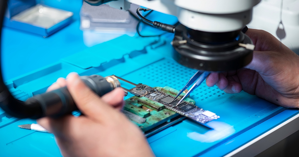
Our project review can cover:
- Rigid PCB reverse engineering
- Flexible PCB and FPC reconstruction
- Rigid-flex PCB structure and documentation reconstruction
- Single-sided, double-sided, and multilayer circuit boards
- Bare PCB samples and fully assembled PCBA samples
- Legacy circuit boards with missing manufacturing files
- Damaged or obsolete boards requiring replacement documentation
- PCB redesign and manufacturability improvement projects
- Prototype reproduction after documentation reconstruction
Before quotation, we confirm the available sample condition, required output files, acceptable inspection method, quantity of samples, expected accuracy, and whether destructive analysis is permitted.
Non-Destructive PCB Reverse Engineering
Non-destructive reverse engineering is suitable when the sample board must remain intact or when only external layers, component information, dimensions, interfaces, and accessible circuit connections need to be reconstructed.
The process may include:
- High-resolution board photography and image alignment
- Board outline, hole, slot, connector, and mechanical measurement
- Component reference, marking, package, and polarity identification
- Continuity testing and accessible net mapping
- External copper-trace and pad reconstruction
- Connector pinout and interface identification
- Visible via and plated-hole location mapping
- Initial schematic and functional-block analysis
- BOM preparation based on identifiable components
Non-destructive methods can preserve the sample, but they may not reveal all internal-layer traces, buried vias, inner-plane structures, hidden connections, or complete multilayer stack-up details.
Destructive PCB Reverse Engineering
Destructive reverse engineering may be required when a multilayer PCB contains internal signal layers, buried vias, blind vias, hidden copper planes, inaccessible traces, or stack-up information that cannot be confirmed through external inspection alone.
Depending on project requirements, the analysis may involve:
- Component removal and board cleaning
- Controlled layer removal or de-layering
- Internal copper-layer imaging
- Cross-section or microsection inspection when required
- Blind-via, buried-via, and plated-hole structure analysis
- Multilayer stack-up estimation
- Internal trace and reference-plane reconstruction
- Layer-to-layer registration and net verification
Destructive analysis may permanently damage the sample. Projects involving multilayer reconstruction should therefore include enough samples for inspection, verification, and functional comparison whenever possible.
Available Documentation and Deliverables
Deliverables are defined according to the quotation scope. Not every project requires every output file, and the final deliverable package depends on the available sample, circuit complexity, inspection method, and verification requirements.
Available outputs may include:
- Gerber or ODB++ manufacturing data
- NC drill and routing files
- PCB fabrication drawing
- Board outline and mechanical dimension drawing
- Layer stack-up documentation
- Altium Designer PCB source files when included in the scope
- Schematic redrawing and circuit documentation
- BOM with component references, packages, and available part information
- Netlist or connectivity documentation
- Pick-and-place or centroid data when applicable
- Assembly drawing and component-location documentation
- Connector pinout and interface definition
- Test-point and electrical verification information
- Redesign recommendations for obsolete or unavailable components
- DFM feedback for prototype or production preparation
PCB Reverse Engineering Workflow
A clearly defined scope is essential because reconstructing a board for dimensional replacement is different from reconstructing a complete verified design package for manufacturing.
- Initial project review: We review sample photographs, board type, layer count, dimensions, available documentation, required outputs, and authorization status.
- Quotation and scope confirmation: The inspection method, number of samples, destructive or non-destructive requirements, deliverables, lead time, and verification level are confirmed.
- Sample inspection: The board is photographed, measured, identified, and documented before further analysis.
- Circuit and layout reconstruction: Components, nets, traces, holes, layers, mechanical features, and assembly information are reconstructed according to the agreed scope.
- Engineering verification: Reconstructed files are checked for dimensional consistency, connectivity, layer relationships, component placement, and manufacturing feasibility.
- Prototype preparation: When required, the reconstructed data can be reviewed for prototype PCB manufacturing or assembly evaluation.
- Final documentation delivery: The agreed manufacturing, schematic, BOM, mechanical, or assembly files are prepared for customer review.
Information Required for Quotation
To evaluate the project accurately, please provide as much of the following information as possible:
- Clear photographs of both sides of the PCB or PCBA
- Board dimensions and approximate layer count
- Number and condition of available samples
- Whether the sample is functional, damaged, or incomplete
- Whether destructive analysis is permitted
- Required output files and software format
- Required schematic, BOM, Gerber, PCB source, or mechanical data
- Known electrical, functional, or interface information
- Connector pinout or test information when available
- Target prototype or production quantity
- Expected accuracy and verification requirements
- Original files, drawings, manuals, photographs, or partial documentation
- Requirements for obsolete-component replacement or circuit redesign
When the available information is incomplete, send the existing sample photographs and your required deliverables first. We can identify the main technical risks and confirm what additional materials or samples may be needed before formal quotation.
Typical Project Scenarios
- Legacy equipment with missing PCB production files
- Repair replacement for discontinued circuit boards
- Customer-owned boards requiring manufacturing documentation
- Gerber, schematic, or BOM reconstruction from physical samples
- Obsolete-component replacement and controlled PCB redesign
- Prototype reproduction for internal engineering verification
- FPC or rigid-flex circuits with unavailable original layout data
- Conversion of incomplete drawings into usable production files
- Manufacturability improvement before restarting production
Authorization and Project Limitations
FPCFAB accepts PCB reverse engineering projects only for customer-owned boards, properly authorized projects, repair and replacement requirements, internal engineering use, legacy product recovery, or other lawful applications. Customers are responsible for confirming that they have the necessary ownership, authorization, and intellectual property rights for the submitted samples and requested work.
Reverse engineering accuracy depends on sample condition, board complexity, layer count, hidden structures, component availability, accessible test information, and the permitted inspection method. Original design intent, firmware, programmable-device contents, proprietary component data, and undocumented functional behavior may not always be recoverable from a physical board alone.
Why Work With FPCFAB
- Project review based on required deliverables rather than a fixed package
- Support for rigid PCB, FPC, rigid-flex PCB, and assembled-board samples
- Coordination between documentation reconstruction and PCB manufacturing
- Practical communication for overseas engineering and purchasing teams
- Non-destructive and destructive project evaluation
- Support for prototype preparation after data reconstruction
- Clear identification of sample, accuracy, and verification limitations
For reconstructed flexible or rigid-flex designs that require production evaluation, review our Flexible PCB Manufacturing and Rigid-Flex PCB Manufacturing services.
Request a PCB Reverse Engineering Quote
Send us clear board photographs, sample quantity, approximate dimensions, available documentation, required output files, and confirmation of whether destructive inspection is permitted. Our team will review the project scope and respond with the required sample information, technical considerations, and quotation details.