FPC coverlay is not simply the flexible-circuit equivalent of rigid PCB solder mask. A film coverlay becomes part of the mechanical stack-up. Its polyimide film and adhesive influence conductor insulation, finished thickness, pad exposure, adhesive flow, bend strain, surface planarity, assembly clearance, and long-term reliability.
Many coverlay problems are caused by treating the coverlay drawing as a secondary fabrication file. An opening that looks acceptable in CAD may become too small after adhesive squeeze-out, too large after tolerance compensation, or misaligned after material movement and lamination. Abrupt coverlay terminations can also create local stiffness changes near active bend regions.
There is no universal opening expansion, adhesive thickness, or registration tolerance suitable for every flexible printed circuit. The correct design depends on copper thickness, conductor topography, pad pitch, cutting method, lamination process, component assembly, bend condition, shielding, stiffeners, and the required inspection class.
This guide explains how engineering and purchasing teams should define FPC coverlay materials, openings, tolerances, adhesive flow, transition areas, assembly requirements, and acceptance criteria before releasing production data.
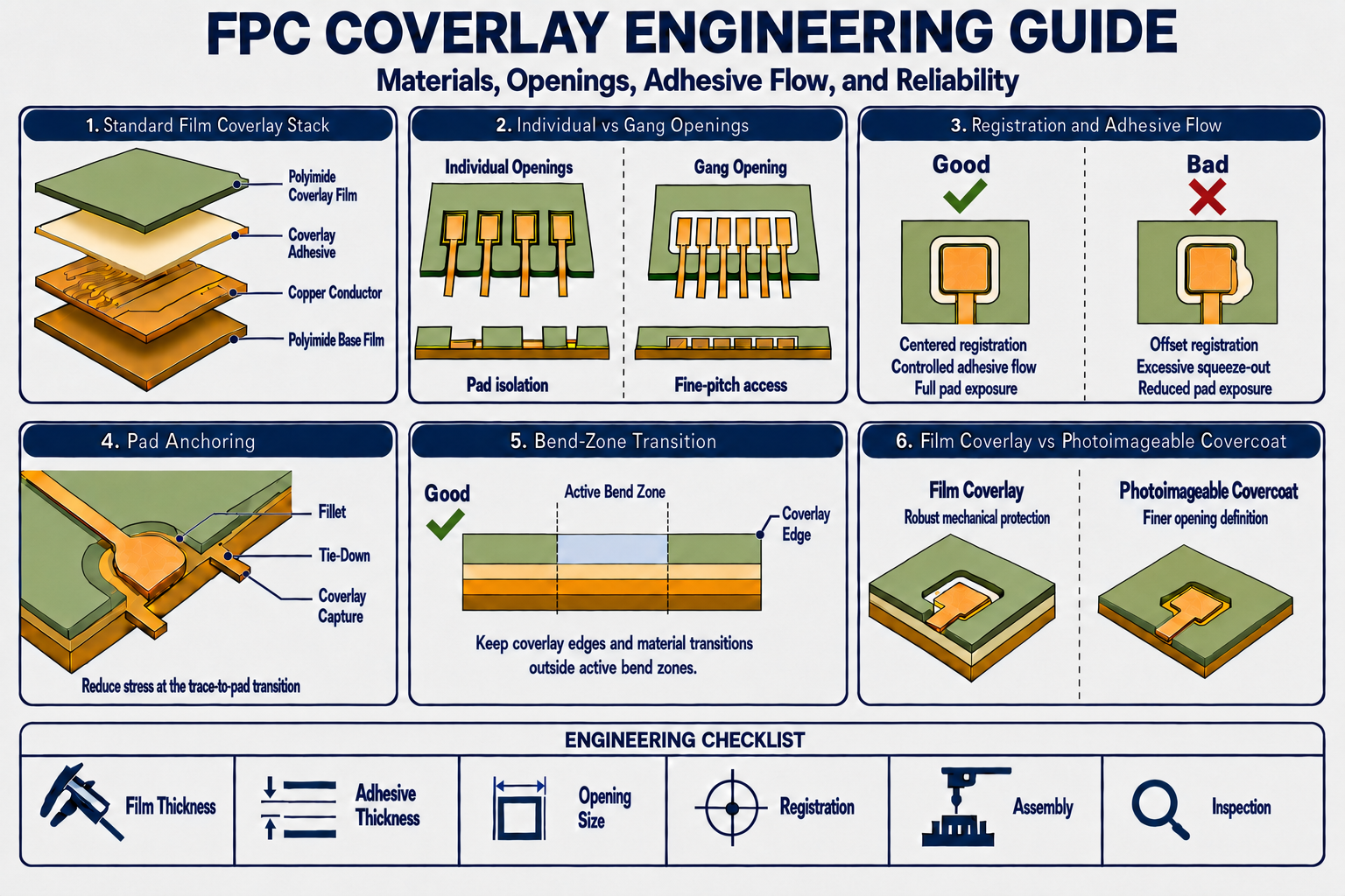
1. What FPC Coverlay Controls
A conventional film coverlay consists of a dielectric film, normally polyimide, coated with a thermosetting adhesive. During lamination, the adhesive softens and flows around the etched conductor pattern before curing.
The coverlay performs several functions:
- Electrically insulates the conductor pattern
- Protects copper from handling and environmental exposure
- Encapsulates conductor edges and surface topography
- Defines exposed pads, test points, contact fingers, and termination areas
- Supports pad necks and copper anchoring features
- Contributes to the finished dielectric thickness
- Affects flexibility and strain distribution
- Influences soldering, cleaning, coating, and assembly access
Because the coverlay is part of the finished construction, it should be reviewed together with the copper pattern, fabrication drawing, assembly drawing, stiffeners, shielding, and mechanical installation data. General layout requirements are discussed in our FPC Design Guidelines.
2. Coverlay, Covercoat, and Solder Mask Terminology
Film Coverlay
Film coverlay, also called coverfilm or cover sheet, normally uses polyimide film with a separate adhesive layer. Openings are produced before lamination by mechanical tooling, laser cutting, or another approved conversion process.
Film coverlay is widely used because it provides robust mechanical protection and is compatible with many static-flex, installation-flex, and dynamic-flex applications.
Photoimageable Covercoat
A photoimageable covercoat is applied and patterned by an imaging process. It can provide finer opening definition than mechanically processed film coverlay and may be considered for dense SMT areas, fine-pitch components, or geometries where coverlay webs are not practical.
Photoimageable covercoat and film coverlay are not automatically interchangeable. Their cured thickness, flexibility, adhesion, thermal capability, chemical resistance, and suitability for repeated bending must be reviewed against the application.
Solder Mask on Rigid-Flex Constructions
Rigid-flex designs may use conventional solder mask on rigid sections and film coverlay over flexible sections. The transition between the two systems must be defined. Uncontrolled overlap, gaps, or material buildup near the rigid-to-flex interface can create assembly and reliability problems.
IPC identifies IPC-2223 as the sectional design standard for flexible printed boards. Adhesive-coated dielectric films used as cover sheets are addressed by IPC-4203. The applicable customer drawing, material specification, and performance class remain the controlling requirements for each project.
3. Typical FPC Coverlay Construction
A basic film-coverlay construction is arranged as follows:
- Polyimide coverlay film
- Coverlay adhesive
- Etched copper conductor pattern
- Flexible copper-clad laminate
For a double-sided FPC, a coverlay is normally laminated to each side. Multilayer and rigid-flex constructions may also include bondply, shielding film, copper reference planes, local stiffeners, pressure-sensitive adhesive, and selective openings.
The nominal film and adhesive values do not directly equal the final local thickness. Adhesive moves during lamination and fills spaces between conductors. Finished thickness therefore varies between copper-covered and copper-free areas.
| Material Element | Common Nominal Options | Engineering Effect |
|---|---|---|
| Polyimide film | 12.5 µm, 25 µm, or 50 µm | Changes insulation, handling strength, finished thickness, and bending stiffness |
| Coverlay adhesive | Approximately 15–50 µm, depending on the material system | Controls conductor encapsulation, adhesive flow, opening contamination risk, and total thickness |
| Copper conductor | Base copper plus any plated buildup | Determines the surface topography that the adhesive must fill |
These values represent common commercial material ranges, not universal design limits. The selected material system and supplier data sheet should be confirmed before the stack-up is released.
4. Selecting Film and Adhesive Thickness
Coverlay film thickness is selected from the electrical insulation, mechanical protection, bending, handling, and finished-thickness requirements. A thinner film can reduce bending stiffness, while a thicker film can provide greater physical protection at the cost of increased total thickness.
Adhesive thickness must be sufficient to fill the etched copper profile and bond to the underlying dielectric. The review should account for:
- Base and finished copper thickness
- Conductor width, spacing, and copper distribution
- Single-sided or double-sided coverlay
- Local plated copper buildup
- Large copper-free areas
- Lamination pressure and temperature
- Required dielectric thickness
- Assembly and operating temperature
- Static or dynamic flexing condition
Adhesive that is too thin may leave voids beside conductors or provide inadequate encapsulation. Excessive adhesive increases finished thickness and can produce greater squeeze-out into pads, fingers, holes, and profile edges.
The complete material relationship is explained in our FPC Stack-Up Design Guide.
5. FPC Coverlay Opening Design
The coverlay artwork should identify every area that must remain exposed after lamination. Typical openings include SMT pads, through-hole pads, contact fingers, test pads, grounding areas, fiducials, tooling features, and selected vias.
Opening geometry must include manufacturing tolerance and expected adhesive flow. Copying rigid-board solder-mask expansion values into an FPC design is not a reliable method because film coverlay has different conversion, registration, and lamination behavior.
| Feature | Coverlay Design Review |
|---|---|
| SMT pads | Confirm individual or gang openings, pad exposure, adhesive squeeze-out allowance, paste printing, and component pitch |
| Plated through-hole pads | Maintain sufficient exposed land and account for opening registration relative to the drilled and plated feature |
| ZIF contact fingers | Use a controlled gang-opening termination and coordinate it with surface finish, stiffener position, outline registration, and insertion thickness |
| Test pads | Provide enough probe access after adhesive flow and dimensional tolerance |
| Vias | Clearly identify whether vias are exposed, covered, or filled; do not rely on an undocumented default |
| Grounding areas | Coordinate the opening with shielding-film termination, conductive adhesive, plating, and assembly contact requirements |
Individual Openings
Individual openings can isolate adjacent pads and provide greater insulation between features. They require enough coverlay web width to survive cutting, handling, alignment, and lamination.
If the remaining web is too narrow, it may shift, wrinkle, tear, or fail to bond consistently. Fine-pitch areas should be reviewed against the manufacturer’s actual coverlay registration and minimum-web capability.
Gang Openings
A gang opening exposes a complete group of pads or contact fingers. It is often used where individual coverlay webs would be too narrow or where a component footprint requires an open assembly area.
The gang opening must not expose unnecessary trace length or allow its edge to terminate at a high-stress conductor transition. Copper necks may require fillets, teardrops, or anchoring features.
6. Registration Tolerance and Opening Compensation
Coverlay registration is affected by more than the cutting accuracy of the opening. The final tolerance includes material conversion, artwork compensation, tooling or laser accuracy, panel handling, polyimide dimensional movement, lamination alignment, heat and pressure, and final profiling.
Many standard-production designs begin with approximately 0.10–0.20 mm of opening compensation per side, but this range must not be treated as a guaranteed rule. Fine-pitch, small-pad, HDI, laser-processed, and high-reliability designs require a supplier-specific review.
The released fabrication drawing should clearly distinguish among:
- Nominal copper-pad dimensions
- Nominal coverlay-opening dimensions
- Permitted opening-location tolerance
- Minimum acceptable pad exposure
- Maximum permitted trace exposure
- Adhesive squeeze-out limit
- Critical connector or component requirements
A tolerance should protect the functional requirement without unnecessarily restricting the manufacturing process. Specifying zero adhesive flow or an unrealistically tight general registration tolerance can increase cost and reduce yield without improving product performance.
7. Adhesive Flow and Squeeze-Out
Coverlay adhesive must flow during lamination. Controlled flow fills the spaces beside conductors and develops a continuous bond. The engineering objective is not to eliminate flow, but to control where it is acceptable and where it interferes with function.
Excessive adhesive squeeze-out may cause:
- Reduced exposed-pad dimensions
- Contamination of contact fingers or test points
- Uneven solderable surfaces
- Interference with wire bonding, conductive adhesive, or connector contact
- Blocked tooling or mounting holes
- Irregular profile edges
- Uncontrolled local thickness
Insufficient adhesive flow may produce voids, incomplete conductor-edge encapsulation, poor bonding in low-copper areas, or delamination during thermal exposure.
The coverlay opening and adhesive-flow criteria should be evaluated after lamination, not only from the pre-lamination film artwork. Critical gold fingers, fine-pitch pads, grounding contacts, and optical or sensor interfaces should have explicit finished-product requirements.
8. Pad Anchoring, Fillets, and Trace Transitions
Flexible copper is vulnerable where a narrow trace enters a larger pad. A sharp change in copper width concentrates strain, particularly when the pad is close to a bend, connector, or unsupported termination.
Common reinforcement features include:
- Fillets at trace-to-pad junctions
- Teardrop transitions
- Copper tie-downs or anchoring spurs
- Rounded copper geometry
- Controlled coverlay overlap around the pad neck
- Local stiffener support where mechanically required
Tie-downs, sometimes called anchoring spurs or rabbit ears, extend beyond the main pad and are captured beneath the coverlay. They can improve resistance to pad lifting when the termination experiences insertion, soldering, or handling load.
These features must be coordinated with electrical spacing, opening geometry, solderability, and the actual direction of mechanical load. Adding copper without reviewing strain can create a new stiffness transition rather than solve the original problem.
9. Coverlay Design in Bend Regions
Coverlay film and adhesive add thickness to the active flex region. Greater thickness increases bending strain and can shift the neutral axis when the construction is asymmetrical.
For demanding bend regions:
- Keep the construction as thin as the electrical and environmental requirements allow
- Avoid unnecessary coverlay overlaps
- Keep openings, pad edges, and rigid features outside the active bend zone
- Avoid abrupt coverlay termination inside the moving area
- Maintain a gradual transition between different material thicknesses
- Coordinate coverlay with shielding-film and stiffener edges
- Review the stack-up for mechanical balance
- Validate the actual bend radius and cycle requirement
Film coverlay may be suitable for dynamic-flex applications, but the result depends on the complete construction. Copper foil type, finished copper thickness, bend direction, routing geometry, adhesive system, shielding, movement path, and cycle count remain part of the evaluation.
Detailed mechanical guidance is available in our FPC Bend Radius Design Guide.
10. FPC Coverlay Requirements for FPCA
When components are mounted on the flexible circuit, coverlay design directly affects solder-paste printing, component placement, solder-joint formation, inspection, cleaning, and rework.
The assembly review should include:
- Individual or gang openings for each component footprint
- Coverlay clearance from SMT pads
- Adhesive squeeze-out near solderable surfaces
- Minimum coverlay web between adjacent openings
- Local flatness under components
- Stiffener support beneath assembly regions
- Solder-paste stencil relationship
- Reflow-temperature compatibility
- Moisture handling and prebaking requirements
- Inspection access and rework clearance
Fine-pitch footprints may not tolerate the same film-coverlay registration used for larger components. A gang opening, photoimageable covercoat, or a revised pad arrangement may be required. The solution should be agreed before stencil fabrication and component assembly.
For projects requiring fabrication and component mounting, see our Flexible PCB Assembly / FPCA service.
11. Stiffeners, Shielding, and Local Material Transitions
Coverlay is often combined with polyimide, FR4, or metal stiffeners; conductive shielding film; copper shields; pressure-sensitive adhesive; and connector reinforcement. Each additional material creates a local thickness and stiffness change.
Stiffener Transitions
A stiffener edge should not terminate inside an active bend region. Coverlay and stiffener termination lines should be coordinated so that a narrow unsupported strip or abrupt step is not created at the same location.
Shielding-Film Grounding
Conductive shielding film may require openings or grounding windows through the coverlay. The design must identify the contact material, grounding method, opening size, adhesive system, and acceptable resistance.
Rigid-Flex Transitions
At a rigid-to-flex transition, coverlay termination, bondply flow, rigid material geometry, copper routing, plated-hole locations, and solder-mask overlap must be reviewed together. The flex opening in the rigid material should not be treated as an ordinary coverlay cutout.
12. When to Consider Photoimageable Covercoat
Photoimageable covercoat may be considered when film-coverlay webs, opening registration, or tooling capability cannot support the required feature density.
Typical review conditions include:
- Fine-pitch SMT pads
- Dense component areas
- Small individual openings
- Complex opening geometry
- High opening-count designs
- Locations requiring tighter image definition
The change should not be made from geometry alone. Confirm the cured covercoat thickness, flexibility, adhesion, environmental resistance, assembly temperature, UL requirement, and compatibility with the intended bend condition.
13. Coverlay Conversion and Lamination Processes
The selected manufacturing method affects opening geometry, edge condition, tooling cost, registration, and lead time.
| Process | Typical Application | DFM Consideration |
|---|---|---|
| Mechanical punching or steel-rule tooling | Repeat production with suitable opening sizes and geometry | Tooling cost, minimum web, corner radius, dimensional change, and production volume |
| Laser cutting | Prototype, low volume, complex outlines, and smaller features | Edge quality, heat effect, residue control, processing time, and material type |
| Photoimageable processing | Fine-pitch or high-density opening patterns | Material qualification, cured thickness, imaging capability, and flex performance |
Lamination must provide uniform pressure and temperature across the panel while allowing the adhesive to fill the copper pattern. Uneven copper distribution, large open areas, tooling features, panel borders, and stacked material transitions can affect the result.
Manufacturer DFM review should be completed before hard tooling is ordered. Late changes to opening dimensions or panel compensation can otherwise add cost and delay production.
14. Common Coverlay Defects and Engineering Causes
| Observed Condition | Possible Cause | Engineering or Process Review |
|---|---|---|
| Opening misregistration | Material movement, tooling error, insufficient compensation, or lamination shift | Review tolerance stack, fiducials, panel compensation, and opening process |
| Adhesive on pads or fingers | Excessive flow, undersized opening, high lamination pressure, or incorrect adhesive selection | Review opening enlargement, adhesive thickness, flow characteristics, and lamination parameters |
| Voids beside conductors | Insufficient adhesive flow, thick copper, contamination, or poor lamination contact | Review adhesive thickness, conductor density, surface preparation, and lamination cycle |
| Blistering or delamination | Moisture, contamination, incomplete cure, inadequate bonding, or excessive thermal exposure | Review material storage, cleaning, prebaking, cure condition, and assembly profile |
| Wrinkles or trapped folds | Handling distortion, uneven lamination pressure, poor tooling, or large unsupported film areas | Review panel tooling, lay-up method, coverlay thickness, and lamination support |
| Cracking near a bend | Excessive thickness, tight radius, abrupt termination, or unsuitable material construction | Review active bend zone, stack-up, material transition, and flex validation |
| Pad lifting | Insufficient anchoring, high soldering or insertion load, poor trace transition, or local flexing | Add fillets or tie-downs where appropriate and review stiffener support |
A visible defect does not always identify the root cause. Cross-sectioning, adhesion testing, dimensional measurement, material traceability, thermal-history review, and process records may be required before corrective action is approved.
15. Inspection and Acceptance Requirements
The acceptance plan should match the product class, application, and drawing requirements. IPC-6013 provides qualification and performance requirements for flexible printed boards, while IPC-A-600 provides visual interpretation of printed-board acceptance conditions. Customer-specific criteria may add tighter or different controls.
Coverlay inspection may include:
- Opening size and location
- Pad and contact-finger exposure
- Adhesive squeeze-out
- Coverlay-to-outline registration
- Voids, wrinkles, blisters, and delamination
- Coverlay damage or exposed copper
- Bonding around conductor edges
- Finished local thickness
- Thermal-stress or soldering resistance
- Adhesion or peel evaluation where specified
- Electrical insulation and continuity testing
Critical dimensions should be identified on the released drawing. A general note such as “coverlay per Gerber” does not define the permitted adhesive intrusion, minimum pad exposure, or connector-interface requirement.
16. Information Required for Coverlay Review and Quotation
Provide the following information whenever available:
- Coverlay artwork or ODB++ data
- Fabrication drawing with critical opening dimensions
- Polyimide film and adhesive thickness
- Material manufacturer or approved equivalent requirement
- Finished copper thickness
- Individual or gang-opening requirements
- Permitted opening-registration tolerance
- Maximum adhesive squeeze-out in critical areas
- Surface finish and exposed contact requirements
- SMT component and connector data
- Stiffener, shielding, and PSA drawings
- Static or dynamic bend conditions
- Assembly temperature and number of reflow cycles
- Inspection class and special documentation
- Prototype and production quantities
If the coverlay construction is not finalized, provide the copper thickness, pad geometry, component pitch, bend condition, stack-up, assembly process, and application environment. The manufacturer can then propose a preliminary material and opening strategy for review.
For a broader quotation-data checklist, read How to Prepare an FPC RFQ.
FPC Coverlay DFM Checklist
| Review Area | Questions to Confirm |
|---|---|
| Material | Are the polyimide film, adhesive system, thickness, temperature rating, and approved equivalents defined? |
| Copper profile | Can the selected adhesive thickness fill the finished copper topography? |
| Openings | Are individual and gang openings suitable for pad pitch, tooling, registration, and assembly? |
| Tolerance | Are finished opening dimensions, location tolerance, pad exposure, and trace exposure controlled? |
| Adhesive flow | Are squeeze-out limits defined for pads, fingers, holes, test points, and grounding contacts? |
| Pad reliability | Are fillets, teardrops, tie-downs, and local stiffeners used where mechanically justified? |
| Bend regions | Are coverlay openings and abrupt terminations outside the active bend zone? |
| Assembly | Are coverlay openings compatible with paste printing, placement, soldering, cleaning, inspection, and rework? |
| Transitions | Are stiffener, shielding, PSA, and rigid-flex termination lines coordinated? |
| Inspection | Are acceptance class, critical dimensions, defect criteria, and required reports specified? |
How FPC Coverlay Affects Cost and Lead Time
Coverlay cost is influenced by material type, film and adhesive thickness, opening count, feature size, cutting process, registration tolerance, tooling, lamination complexity, inspection, and order volume.
Cost and lead time may increase when the design requires:
- Uncommon material constructions
- Fine individual openings and narrow coverlay webs
- Tight opening-registration tolerances
- Multiple coverlay types on one circuit
- Laser processing with a high opening count
- Photoimageable covercoat qualification
- Critical adhesive-flow limits
- Several stiffeners, shields, or local reinforcement layers
- Special inspection, coupons, testing, or traceability
Gang openings, standard material options, realistic tolerances, and early DFM review can reduce unnecessary tooling and yield risk. Functional connector, assembly, insulation, and flex requirements should not be relaxed solely to lower the initial quotation.
How FPCFAB Supports Coverlay Design and Production
FPCFAB reviews coverlay material, film and adhesive thickness, opening geometry, registration, adhesive flow, copper topography, pad anchoring, bend regions, shielding, stiffeners, connector areas, and FPCA requirements before production.
Our Flexible PCB Manufacturing service supports single-sided, double-sided, and multilayer FPC projects from prototype and NPI through pilot-run and production.
Customers may provide completed production data or request an FPC Design & DFM Review before finalizing materials, openings, tolerances, and assembly details.
Conclusion
Reliable FPC coverlay design requires more than selecting a polyimide film and drawing openings around pads. Film thickness, adhesive thickness, copper topography, opening geometry, registration, adhesive flow, pad anchoring, bend strain, stiffener transitions, shielding, and assembly must be evaluated as one construction.
The fabrication drawing should define the finished functional requirements while allowing a realistic manufacturing tolerance. Critical pad exposure, contact fingers, connector regions, grounding windows, and bend transitions deserve separate controls rather than one general coverlay note.
Send your Gerber or ODB++ data, fabrication drawing, stack-up, coverlay requirements, assembly information, quantities, and application conditions to FPCFAB for engineering review and quotation support.