Flexible printed circuits are widely used in compact electronic assemblies where space, weight, routing flexibility, and mechanical integration are critical. However, a flexible circuit cannot be designed in exactly the same way as a rigid printed circuit board. Its long-term reliability depends not only on electrical performance, but also on how the circuit responds to bending, folding, vibration, thermal cycling, and assembly stress.
Effective FPC design guidelines must therefore consider materials, copper construction, bend geometry, layer stack-up, coverlay openings, stiffener locations, via placement, and manufacturing tolerances from the beginning of the project. A design that performs well electrically may still fail during fabrication or field use if mechanical stress is concentrated in the wrong area.
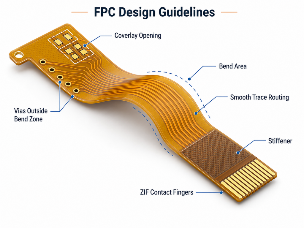
This guide explains the key design factors that influence reliable flexible PCB manufacturing. It is intended for hardware engineers, PCB designers, product development teams, and sourcing professionals working with single-sided, double-sided, and multilayer flexible circuits.
1. FPC Design Guidelines for Circuit Construction
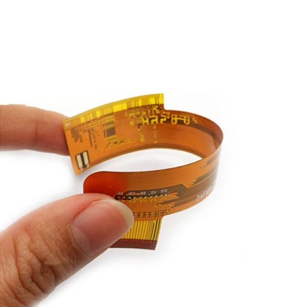
Before defining trace geometry or component placement, designers should first understand the physical construction of the flexible circuit. Unlike a conventional rigid PCB, an FPC is built from thin polymer-based materials that must maintain electrical integrity while remaining mechanically flexible.
A typical flexible PCB construction may include the following elements:
- Polyimide base film: The primary dielectric substrate, selected for its dimensional stability, thermal resistance, and flexibility.
- Rolled annealed or electrodeposited copper: The conductive layer used to form traces, pads, and power paths.
- Adhesive or adhesiveless laminate: The bonding system between copper and polyimide, depending on the material construction.
- Polyimide coverlay: A flexible protective film that insulates and protects the copper circuitry.
- Stiffeners: Local reinforcement materials such as polyimide, FR-4, or stainless steel used under connectors, components, or contact areas.
- Surface finish: Finishes such as ENIG, immersion tin, or OSP applied to exposed pads and contact areas.
The selected material system directly affects flexibility, thickness, bend endurance, thermal performance, impedance control, and manufacturability. For example, rolled annealed copper is generally preferred for dynamic flex applications because its grain structure provides better resistance to repeated bending than standard electrodeposited copper.
Designers should also distinguish between static flex and dynamic flex applications. Static flex circuits are bent mainly during installation and remain in a fixed position during service. Dynamic flex circuits are repeatedly bent during operation and require stricter control of copper type, bend radius, trace orientation, and layer construction.
Defining the application type at the beginning of the design process allows the FPC manufacturer to recommend a suitable material stack-up and avoid unnecessary reliability risks later in production.
2. Bend Radius Design Considerations
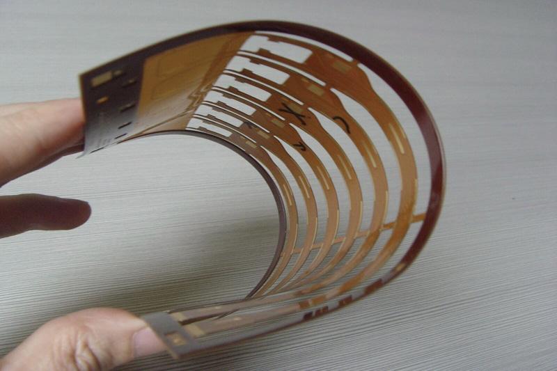
Among the most important FPC design guidelines, bend radius has a direct influence on conductor strain, dielectric stress, and long-term flex reliability. An excessively tight bend can concentrate mechanical strain in the copper conductors and dielectric layers, increasing the risk of trace cracking, coverlay delamination, impedance variation, and premature fatigue failure.
The required minimum bend radius depends on the flex construction, copper thickness, total circuit thickness, number of conductive layers, material type, and whether the application is static or dynamic. As a general design principle, the bend radius should be increased whenever the circuit includes thicker copper, multiple conductive layers, plated through-holes, stiffeners, or repeated flexing.
Static Flex Applications
In a static flex application, the circuit is typically bent during installation and remains in a fixed position during normal operation. These designs can usually tolerate a smaller bend radius than dynamic flex circuits, provided that the bend is formed carefully and does not occur directly across vias, solder joints, stiffener edges, or abrupt changes in copper geometry.
For single-layer and double-layer constructions, a practical starting point is to maintain a bend radius several times greater than the total FPC thickness. More complex multilayer constructions generally require a larger radius because the outer copper layers experience greater tensile and compressive strain during bending.
Dynamic Flex Applications
Dynamic flex circuits are designed to move repeatedly during product operation. Typical applications include printhead assemblies, camera modules, sliding mechanisms, medical devices, robotics, and moving sensor systems.
These applications require a significantly larger bend radius and tighter control of the flex area. Rolled annealed copper is commonly preferred, and the bend region should be kept as thin, balanced, and mechanically uniform as possible. Adhesiveless copper-clad laminate may also be selected when improved flexibility, reduced thickness, and better dimensional stability are required.
Trace Routing Through the Bend Area
Conductors should pass through the bend zone as straight and parallel as possible. Traces should generally be routed perpendicular to the bend axis so that the copper experiences controlled bending rather than twisting or diagonal strain.
- Avoid sharp trace corners inside the bend area.
- Use smooth curves or large-radius routing transitions.
- Avoid sudden trace-width changes in the flex zone.
- Keep vias and plated holes away from the bend region.
- Do not place solder joints or component terminations inside an active flex area.
- Distribute copper evenly to reduce local stiffness differences.
When traces change direction, curved routing is generally more reliable than a sharp 90-degree corner because it reduces stress concentration. If space is limited, two 45-degree transitions may be used, but a smooth arc is preferred for high-flex applications.
Neutral Bend Axis
During bending, the material on the outside of the bend is placed in tension, while the material on the inside is compressed. Between these regions is the neutral bend axis, where mechanical strain is lowest.
For reliable FPC design, critical copper layers should be positioned as close as practical to the neutral bend axis. A symmetrical or balanced stack-up can reduce strain on the conductors, especially in multilayer flexible circuits. Uneven dielectric thickness or asymmetric copper distribution can shift the neutral axis and increase stress on one side of the circuit.
The final bend radius should always be reviewed together with the FPC manufacturer because general design rules cannot replace a construction-specific mechanical assessment. Material thickness, copper type, adhesive system, layer count, and expected flex cycles must all be considered before the design is released for production.
3. Copper Thickness and Conductor Design
Copper thickness has a direct influence on current-carrying capacity, flexibility, etching accuracy, conductor fatigue, and overall FPC thickness. Selecting copper only according to electrical load can create mechanical problems, while selecting copper only for flexibility may result in excessive temperature rise or voltage drop.
Common flexible circuit copper thicknesses include approximately 12 µm, 18 µm, and 35 µm. Thinner copper generally provides better flexibility and lower bending strain, while thicker copper supports higher current but increases stiffness and makes fine-line etching more difficult.
Rolled Annealed Copper and Electrodeposited Copper
The two most common copper types used in flexible circuits are rolled annealed copper and electrodeposited copper.
- Rolled annealed copper: Commonly selected for dynamic flex and repeated-bending applications because its elongated grain structure provides better fatigue resistance.
- Electrodeposited copper: Often used in static flex and cost-sensitive applications where repeated movement is limited.
For applications involving frequent flexing, rolled annealed copper is generally the preferred material. However, copper type should be evaluated together with laminate construction, plating thickness, bend radius, and expected flex cycles.
Trace Width and Current-Carrying Capacity
Trace width should be determined according to current load, allowable temperature rise, copper thickness, conductor length, ambient conditions, and available routing space. Narrow conductors may be suitable for low-current signal lines, but power paths often require wider traces, thicker copper, or local copper reinforcement.
In flexible circuits, current-carrying calculations should not be copied directly from rigid PCB assumptions without review. The thin dielectric construction, limited heat-spreading area, coverlay system, and installation environment can affect thermal performance.
Avoid Abrupt Conductor Transitions
Sudden changes in trace width can create local stress concentration and may also complicate etching control. Where a conductor must transition from a narrow signal trace to a wider pad or power section, use a gradual taper rather than an abrupt step.
- Use smooth conductor-width transitions.
- Avoid sharp internal corners.
- Maintain uniform copper distribution where possible.
- Keep critical narrow traces away from stiffener edges.
- Avoid routing high-stress conductors through repeated bend zones.
Copper Balance and Mechanical Stability
Uneven copper distribution can create local differences in stiffness, thermal expansion, and dimensional stability. This is especially important in double-sided and multilayer FPC constructions, where large copper areas on one layer and sparse routing on another may increase warpage or shift the neutral bend axis.
Where electrical requirements allow, copper should be distributed as evenly as practical across the flex region. Hatched copper may be used instead of solid copper planes in selected areas to reduce stiffness while maintaining shielding, grounding, or current-distribution functions.
Plating Thickness in Flexible Areas
Additional copper plating increases conductor thickness and may reduce flexibility. For this reason, plated copper in dynamic bend regions should be carefully controlled. Vias, plated through-holes, and heavily plated conductors should generally be kept outside active flex zones whenever possible.
The final copper specification should be confirmed with the FPC manufacturer based on required current capacity, minimum trace width and spacing, flex category, surface finish, via structure, and expected product life.
4. FPC Stack-Up Design
The FPC stack-up determines the circuit thickness, flexibility, impedance behavior, mechanical balance, thermal performance, and manufacturing complexity. A well-designed stack-up should satisfy the electrical requirements while keeping the flexible area as thin, symmetrical, and mechanically uniform as possible.
The appropriate construction depends on the required layer count, current capacity, signal density, shielding needs, bend performance, component layout, and final assembly method. Increasing the number of conductive layers generally improves routing capability, but it also increases stiffness and reduces bend endurance.
Single-Sided FPC
A single-sided flexible circuit contains one conductive copper layer on a polyimide substrate, usually protected by coverlay. This construction offers the lowest thickness, excellent flexibility, simple manufacturing, and relatively low cost.
Single-sided FPCs are commonly used in simple interconnects, membrane switches, sensor connections, LED modules, and applications where routing density is limited. They are particularly suitable for designs that require repeated bending and do not need crossovers or complex signal routing.
Double-Sided FPC
A double-sided FPC contains copper circuitry on both sides of the dielectric substrate, with plated through-holes or vias providing electrical interconnection between the layers. This construction supports higher routing density and more complex electrical functions than a single-sided design.
Because double-sided FPCs are thicker and mechanically less flexible, the bend area should be carefully reviewed. Vias should be positioned away from active bend zones, and copper distribution should be balanced between the two sides to reduce warpage and local strain.
Multilayer FPC
Multilayer flexible circuits use three or more conductive layers to support high-density routing, controlled impedance, power distribution, grounding, and electromagnetic shielding. They are commonly used in advanced medical electronics, aerospace systems, communication equipment, camera modules, and compact consumer devices.
Although multilayer FPCs provide greater electrical capability, they require more careful mechanical design. Additional copper and dielectric layers increase total thickness and move the outer conductors farther from the neutral bend axis, which increases tensile and compressive strain during bending.
Whenever possible, multilayer constructions should avoid repeated flexing. If dynamic movement is unavoidable, the bend region should be simplified, thinned, or designed as a dedicated flex section with fewer conductive layers.
Rigid-Flex Construction
Rigid-flex circuits combine rigid PCB sections and flexible interconnect sections in a single integrated structure. They can reduce connector count, save assembly space, improve electrical continuity, and increase system-level reliability.
Rigid-flex stack-up design requires close coordination between the electrical designer and the manufacturer. The transition between rigid and flexible sections must be carefully controlled to avoid stress concentration, resin cracking, copper fatigue, and delamination.
- Keep vias and plated through-holes away from the rigid-to-flex transition.
- Avoid abrupt copper termination at the transition edge.
- Use appropriate coverlay and flexible dielectric termination geometry.
- Apply suitable strain-relief features where required.
- Maintain balanced copper distribution in the rigid sections.
Adhesive and Adhesiveless Constructions
Flexible laminates are available in adhesive-based and adhesiveless constructions. In an adhesive-based laminate, copper is bonded to the polyimide film using an adhesive layer. In an adhesiveless laminate, the copper is directly bonded to the polyimide without a separate adhesive layer.
Adhesiveless constructions generally provide lower thickness, improved dimensional stability, better thermal performance, and enhanced flex endurance. They are often preferred for fine-line circuits, multilayer FPCs, controlled-impedance designs, and dynamic flex applications.
Adhesive-based materials may still be suitable for cost-sensitive static flex applications, but the added adhesive thickness and lower thermal resistance should be considered during stack-up selection.
Stack-Up Symmetry and Thickness Control
A balanced stack-up helps reduce warpage, uneven bending behavior, and mechanical stress. In double-sided and multilayer flexible circuits, copper weight, dielectric thickness, coverlay construction, and reinforcement materials should be distributed as symmetrically as the design allows.
Total FPC thickness should also be controlled carefully because even small increases can significantly reduce flexibility. Designers should avoid unnecessary copper layers, excessive plating, oversized stiffeners, and redundant dielectric layers in active flex regions.
The final stack-up should be reviewed with the FPC manufacturer before layout release. This review should confirm the material system, copper type, dielectric thickness, coverlay construction, finished thickness, impedance requirements, bend category, and manufacturing capability.
5. Via, Hole, and Pad Design for FPC Reliability
Vias, plated through-holes, and component pads are common stress-sensitive features in flexible circuits. Their locations, annular ring dimensions, plating thickness, and relationship to bend areas must be carefully controlled to prevent copper fatigue, barrel cracking, pad lifting, and interconnection failure.
Keep Vias Outside Active Bend Areas
Vias and plated through-holes should generally be kept outside dynamic bend zones. During repeated flexing, the plated barrel and surrounding annular ring are exposed to mechanical strain that can cause cracking at the knee of the hole or separation between the copper plating and base laminate.
If a via must be positioned near a bend region, the bend radius should be increased and sufficient clearance should be provided between the via and the start of the bend. The final spacing should be reviewed against the actual FPC thickness, copper construction, and expected flex cycles.
Use Teardrops at Trace-to-Pad Transitions
Teardrop-shaped copper transitions can improve mechanical robustness where a narrow trace connects to a pad or via. This geometry reduces local stress concentration, increases the effective copper connection area, and provides additional process tolerance for drilling and registration.
Teardrops are particularly useful in flexible circuits because dimensional movement during fabrication can be greater than in rigid PCB production. They should be considered for fine-pitch designs, small annular rings, and areas exposed to assembly or handling stress.
Pad Support and Anchoring
Surface-mount and connector pads should be designed with adequate copper anchoring. Unsupported pads at the edge of a coverlay opening may be more vulnerable to lifting during soldering, connector insertion, rework, or repeated mechanical loading.
- Use sufficient pad-to-trace transition area.
- Avoid narrow neck-down regions immediately beside pads.
- Provide local stiffener support under connectors and components.
- Maintain appropriate coverlay overlap around the pad opening.
- Avoid placing pads directly at the edge of a bend region.
Annular Ring and Drill Tolerance
Hole diameter, finished hole size, drill tolerance, plating allowance, and annular ring must be defined together. Small annular rings can reduce routing space, but they also increase sensitivity to drill wander, material movement, and layer-to-layer registration.
For reliable manufacturing, the minimum annular ring should be selected according to the manufacturer’s proven process capability rather than rigid PCB assumptions alone. Flexible materials can expand or contract during lamination, drilling, and thermal processing, making registration control especially important.
Vias in Pads and Filled Vias
Via-in-pad structures may be used in high-density FPC and rigid-flex designs, but they require additional processing such as resin filling, planarization, and copper capping. These processes increase cost and must be specified clearly in the fabrication documentation.
Unfilled vias placed directly in solder pads can allow solder to wick into the hole, reducing solder joint volume and creating assembly defects. For this reason, via-in-pad designs should be reviewed jointly by the FPC manufacturer and assembly supplier.
6. Coverlay and Stiffener Design
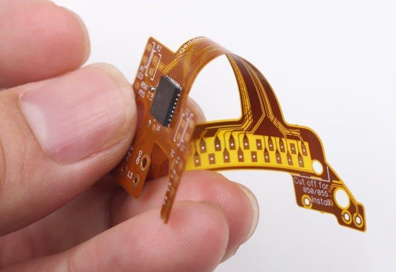
Coverlay and stiffeners are essential mechanical and protective elements in flexible circuit construction. Their thickness, material, opening geometry, adhesive system, and placement can strongly influence assembly yield, bending behavior, connector performance, and long-term reliability.
Coverlay Function and Material Selection
Polyimide coverlay protects the copper circuitry from oxidation, contamination, handling damage, and environmental exposure. It performs a function similar to solder mask on a rigid PCB, but it is a laminated flexible film rather than a liquid photoimageable coating.
Coverlay thickness should be selected according to insulation requirements, copper thickness, flexibility, and dimensional tolerance. Excessively thick coverlay can increase stiffness, while insufficient coverlay thickness may reduce dielectric protection and mechanical durability.
Coverlay Opening Design
Coverlay openings must account for punching or laser-cutting tolerance, lamination movement, adhesive squeeze-out, and registration capability. Openings that are too tight may partially cover pads, while openings that are too large may reduce pad support and expose unnecessary copper.
- Allow sufficient clearance around solderable pads.
- Avoid narrow coverlay webs that may tear or shift during lamination.
- Use rounded opening corners where practical.
- Maintain adequate coverlay overlap on conductor edges.
- Review fine-pitch openings against the manufacturer’s registration capability.
Stiffener Materials
Stiffeners are used to reinforce selected areas without making the entire circuit rigid. Common stiffener materials include polyimide, FR-4, and stainless steel.
- Polyimide stiffener: Provides moderate reinforcement while maintaining a thin profile and good thermal compatibility with the FPC.
- FR-4 stiffener: Commonly used under connectors, components, and soldered regions where greater rigidity is required.
- Stainless steel stiffener: Used where high dimensional stability, strength, wear resistance, or precise thickness control is required.
Stiffener Edge Placement
The edge of a stiffener creates an abrupt transition in local thickness and stiffness. If a conductor bends directly at this edge, mechanical stress can become concentrated and lead to copper fatigue or coverlay cracking.
Critical traces should not change direction at the stiffener boundary. Where possible, the stiffener edge should be positioned away from active bend areas, and a controlled transition or strain-relief feature should be incorporated into the mechanical design.
Connector Finger and ZIF Interface Design
Flexible circuits used with zero insertion force connectors require precise control of contact pitch, finger width, exposed copper length, surface finish, total thickness, stiffener thickness, and edge profile.
The finished thickness at the connector interface must match the connector specification. Excessive thickness may prevent insertion, while insufficient thickness may result in poor contact force or intermittent electrical performance. Hard gold or another suitable contact finish may be required for repeated mating cycles.
7. Controlled Impedance and Signal Integrity
High-speed flexible circuits often require controlled impedance, stable reference planes, low-loss materials, and consistent trace geometry. Unlike rigid PCBs, flexible circuits can change shape during installation and operation, so the mechanical configuration may also influence electrical performance.
Impedance-Related Parameters
Controlled impedance depends on several construction parameters:
- Trace width and copper thickness
- Dielectric thickness
- Dielectric constant of the polyimide and adhesive system
- Distance to the reference plane
- Coverlay thickness and adhesive flow
- Etching tolerance and finished conductor geometry
The FPC stack-up and impedance model should be confirmed before routing is finalized. Nominal dimensions alone are not sufficient because actual finished copper thickness, trapezoidal etch profile, coverlay adhesive, and laminate tolerances can affect the final impedance value.
Reference Plane Design
Solid reference planes provide stable return paths and improved shielding, but they also increase stiffness. In flexible regions, hatched ground planes may be used to reduce mechanical rigidity while maintaining electrical reference and electromagnetic compatibility functions.
The hatch pattern, copper coverage, trace orientation, and return-current path should be evaluated carefully. Excessively open hatching may degrade impedance consistency or shielding performance, while dense hatching may provide limited mechanical benefit.
Differential Pair Routing
Differential pairs should maintain consistent spacing, width, reference-plane relationship, and path length. Abrupt changes in geometry, unsupported plane gaps, sharp corners, and unequal routing through bend regions can introduce impedance discontinuities and timing skew.
For high-speed interfaces, the design should include an impedance requirement, target value, tolerance, test method, and coupon strategy where applicable. These details should be agreed with the manufacturer before fabrication begins.
8. Design for Manufacturability in Flexible PCB Production
Within practical FPC design guidelines, design for manufacturability, commonly referred to as DFM, is the process of evaluating whether an FPC design can be produced consistently, economically, and within the required reliability limits. Early DFM review helps prevent redesign, low yield, dimensional variation, assembly defects, and delayed delivery.
For broader industry guidance on flexible and rigid-flex circuit design, designers may also refer to relevant IPC standards and technical resources published by IPC.
Trace Width and Spacing
Minimum trace width and spacing should be selected according to copper thickness, etching process, circuit size, panel utilization, and required production yield. A geometry that is technically possible may still be unsuitable for stable mass production.
Designers should avoid using the manufacturer’s absolute minimum capability throughout the entire circuit. Providing additional process margin improves yield and reduces sensitivity to etching variation, material movement, and registration tolerance.
Dimensional Stability and Registration
Polyimide materials can expand, shrink, or distort during lamination, drilling, etching, and thermal processing. Multilayer FPCs and rigid-flex circuits are especially sensitive to cumulative registration error.
Critical features such as fine-pitch pads, coverlay openings, stiffener edges, tooling holes, and connector fingers should include realistic manufacturing tolerances. Mechanical drawings should clearly identify datum structures and critical-to-function dimensions.
Panelization and Tooling
Panelization influences material utilization, handling stability, assembly efficiency, and final part accuracy. Small or irregular flexible circuits may require support frames, breakaway tabs, temporary carriers, or dedicated tooling to remain stable during fabrication and assembly.
Panel format should be coordinated with both the FPC manufacturer and the assembly provider. Poor panel design can lead to excessive movement, solder paste misregistration, pick-and-place instability, and damage during depanelization.
Surface Finish Selection
Surface finish should be selected according to solderability, connector requirements, storage life, wire bonding, contact wear, and assembly temperature. Common finishes include ENIG, immersion tin, OSP, and hard gold for edge contacts.
The finish thickness and application area should be specified clearly. For connector fingers, the contact finish must be compatible with the intended mating cycles and connector system.
Fabrication Documentation
Complete fabrication data should include more than Gerber or ODB++ files. A reliable FPC package should also define the stack-up, material type, copper thickness, coverlay construction, stiffener material, finished thickness, surface finish, impedance requirements, bend category, dimensional tolerances, and testing requirements.
- Clearly identify static and dynamic flex regions.
- Define critical bend direction and bend radius.
- Specify connector-interface thickness.
- Provide controlled-impedance requirements where applicable.
- State electrical test and inspection requirements.
- Include a mechanical drawing with critical dimensions and tolerances.
9. Common FPC Design Mistakes
Many flexible circuit failures can be traced back to design decisions made before fabrication. The following issues are among the most common causes of manufacturing difficulty and field reliability problems.
Using Rigid PCB Rules Without Mechanical Review
A flexible circuit is not simply a thin rigid PCB. Applying rigid-board routing, via placement, pad geometry, and copper-plane practices without considering bending behavior can create high-stress regions and premature conductor failure.
Insufficient Bend Radius
An overly tight bend increases strain in copper and dielectric materials. This risk becomes greater with thicker copper, multilayer constructions, plated features, and repeated movement.
Vias Inside the Flex Zone
Plated holes placed in dynamic bend areas are vulnerable to barrel cracking and annular ring fatigue. Vias should be relocated to stable sections whenever the layout permits.
Sharp Corners and Abrupt Trace Transitions
Sharp geometry concentrates mechanical stress and can also create etching irregularities. Smooth curves, tapered transitions, and teardrops provide better mechanical continuity.
Poor Copper Balance
Large differences in copper coverage can produce uneven stiffness, warpage, and an unstable neutral bend axis. Balanced conductor distribution should be maintained where practical.
Incorrect Stiffener Placement
Stiffener edges placed directly under bend points or critical traces can create localized strain. Stiffeners should support connectors and components without shifting the mechanical stress into an adjacent unreinforced region.
Overlooking Assembly Requirements
Component placement, soldering temperature, reflow support, panel handling, connector insertion, and depanelization should be considered during the FPC design stage. A circuit that is fabricable may still be difficult to assemble reliably.
10. FPC Design Review Checklist
Before releasing a flexible circuit for production, designers should complete a structured review covering electrical, mechanical, material, and manufacturing requirements.
- Confirm whether the application is static flex or dynamic flex.
- Verify the minimum bend radius and bend direction.
- Keep vias, plated holes, solder joints, and components outside active bend zones.
- Use appropriate copper type and copper thickness.
- Maintain smooth trace geometry through flex regions.
- Review copper balance and neutral-axis location.
- Confirm the layer stack-up and finished thickness.
- Define coverlay openings and registration tolerances.
- Review stiffener material, thickness, and edge location.
- Confirm connector-finger thickness and surface finish.
- Validate controlled-impedance requirements.
- Check minimum trace width, spacing, annular ring, and drill capability.
- Coordinate panelization with fabrication and assembly requirements.
- Provide complete fabrication drawings and material specifications.
- Request a manufacturer DFM review before production release.
Conclusion
Reliable flexible PCB manufacturing begins with FPC design guidelines that account for both electrical performance and mechanical behavior. Bend radius, copper type, conductor geometry, layer stack-up, via placement, coverlay, stiffeners, impedance control, and manufacturing tolerances must be considered as an integrated system.
The most effective FPC design guidelines are not based on a single fixed rule. They depend on the material system, total thickness, flex category, assembly process, operating environment, and expected product life. Early collaboration with an experienced FPC manufacturer can identify risk areas before tooling and production begin.
FPCFAB supports flexible PCB manufacturing and flexible PCB assembly for prototype and production projects. Our team can review your design data, stack-up requirements, bend conditions, material selection, stiffener structure, and manufacturing tolerances before production.
For additional background, read What Is FPC Manufacturing? to understand the complete fabrication process, and compare design options in Flexible PCB vs Rigid PCB.
When preparing a project for quotation, use our FPC RFQ Requirements guide to confirm the required Gerber data, fabrication drawing, stack-up, materials, quantities, testing requirements, lead time, and FPCA files.
For more information about our manufacturing capabilities, visit our Flexible PCB Manufacturing and Flexible PCB Assembly / FPCA service pages.