FPC EMI shielding is not a separate accessory that can be added after the circuit layout is complete. The shield becomes part of the flexible-circuit construction and changes thickness, stiffness, grounding, heat flow, controlled impedance, assembly clearance, and bend performance.
A note such as “add EMI film” is therefore not a complete engineering requirement. The drawing must identify where shielding is required, which nets or reference planes provide the ground connection, how the shield is terminated, where openings are permitted, and whether the circuit will be folded once or flexed repeatedly in service.
The correct construction depends on the interference source, frequency range, required attenuation, available ground structure, circuit geometry, environmental exposure, and mechanical duty. A shield that performs well on a flat test coupon may behave differently after forming, connector installation, or repeated bending.
This guide covers the principal shielding methods used on flexible printed circuits, including conductive shielding films, bonded copper foil, conductive coatings, and internal copper reference layers. It also addresses grounding, shield coverage, openings, bend-zone transitions, inspection, and the information needed for quotation and production release.
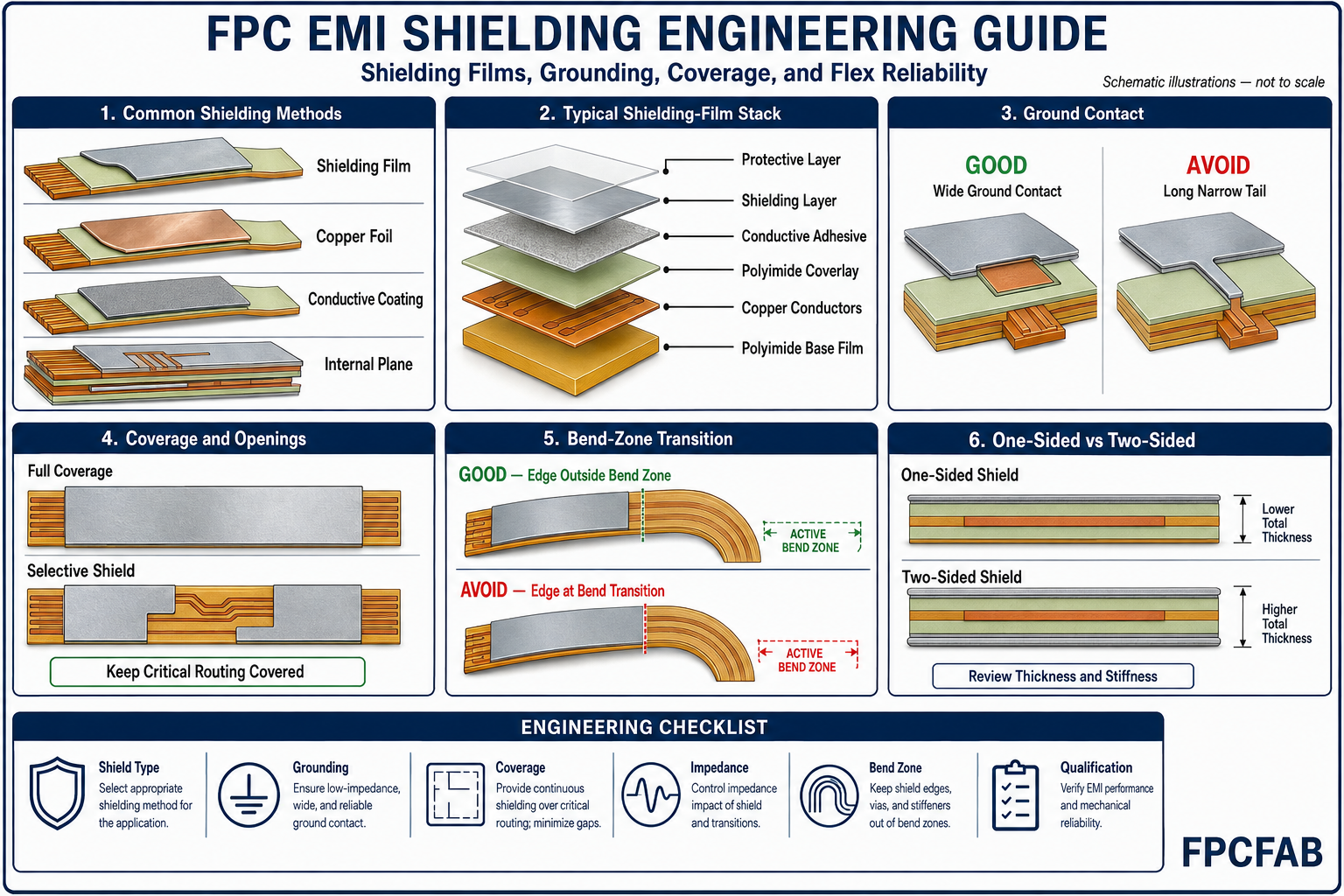
1. What FPC EMI Shielding Controls
An FPC shield may be used to reduce radiated emissions from the circuit, limit susceptibility to an external field, or reduce coupling between adjacent signal groups. These objectives are related, but they are not interchangeable. The required construction should be based on the EMC problem that must be controlled.
In practical designs, the shield also affects:
- return-current continuity and reference-plane stability;
- electric-field and magnetic-field coupling;
- common-mode current and cable radiation;
- single-ended and differential impedance;
- crosstalk between signal groups;
- finished thickness, minimum bend radius, and flex life;
- heat dissipation, moisture protection, and assembly access.
The shield should consequently be reviewed with the complete FPC stack-up, not evaluated as an isolated material layer.
2. Shielding, Grounding, and Return Path Are Different Functions
A conductive layer does not provide useful shielding merely because it is present. It must be connected to an appropriate reference with sufficiently low impedance over the frequency range of interest. A long, narrow grounding tail may show continuity on a multimeter while performing poorly at high frequency because its inductance dominates the connection.
The signal return path must also be considered separately. High-speed current follows the path of lowest impedance, which is normally close to the signal conductor when a continuous reference plane is available. If the reference is interrupted by slots, neck-downs, openings, or connector transitions, return current may spread into the shield or enclosure and increase common-mode radiation.
Grounding strategy should therefore define:
- the intended ground net and chassis relationship;
- the number and position of shield-ground connections;
- the connection method at connectors and rigid-board interfaces;
- whether the shield is grounded at one end, both ends, or at multiple points;
- how ESD current is routed without crossing sensitive circuitry.
There is no universal rule that every cable shield should be grounded at only one end or always at both ends. The correct arrangement depends on frequency, grounding architecture, safety requirements, common-mode current, and the equipment-level EMC design.
3. Common FPC Shielding Constructions
Several shielding constructions are used in production. They differ in conductivity, flexibility, thickness, coverage, processing, and cost.
Conductive EMI Shielding Film
A flexible shielding film is commonly laminated over the coverlay. Depending on the product, it may combine a protective layer, metallic or conductive shielding layer, and conductive adhesive. Selected areas of the coverlay are opened so that the conductive adhesive can contact exposed ground pads or grounding traces.
This construction is thin and suitable for complex outlines, but performance depends on material grade, lamination conditions, grounding geometry, surface preparation, and bend duty. The film supplier’s shielding-effectiveness, adhesion, environmental, and flex data should be reviewed for the intended application.
Bonded Copper Foil Shield
Copper foil provides high conductivity and can form a robust ground or shielding layer. It is normally bonded with an adhesive system and selectively connected to ground. Copper thickness, foil temper, adhesive thickness, pattern geometry, and local plating all influence stiffness and fatigue behavior.
A solid copper shield may be unsuitable in an active flex region. Cross-hatched or selectively patterned copper can reduce stiffness, but the resulting aperture geometry changes current distribution and shielding performance. The pattern must be evaluated against the actual EMC and mechanical requirements.
Conductive Ink or Coating
Silver-filled or other conductive coatings can provide lightweight, selective coverage and are useful for certain low-profile constructions. Their electrical resistance, adhesion, cracking behavior, environmental stability, and termination method vary by material system. They should not be treated as equivalent to a continuous copper plane.
Internal Copper Reference Plane
In a multilayer FPC or rigid-flex circuit, an internal copper plane can provide a controlled signal reference and may also contribute to EMI control. It offers close coupling to signal conductors, but adds copper and dielectric layers to the stack-up. Plane segmentation, flex-zone copper pattern, layer balance, and via connections require careful review.
4. How an EMI Shielding Film Is Integrated
A typical shielded FPC may contain the base film, etched copper conductors, coverlay adhesive, polyimide coverlay, and an externally laminated EMI shielding film. The coverlay remains the primary conductor-insulation layer; the shielding film is applied over it and reaches ground through defined contact openings.
The ground-contact area requires enough exposed metal to accommodate coverlay registration, shielding-film registration, material movement, and conductive-adhesive flow. A nominal CAD overlap with no tolerance allowance can produce intermittent contact after lamination.
The design should also distinguish between a ground-contact opening and a normal component-pad opening. The former must support stable electrical contact under the shield, while the latter may need solderability, probe access, or assembly clearance. The coverlay drawing should clearly identify both functions.
5. Engineering Comparison of Shielding Options
| Review Area | Shielding Film | Copper Foil Shield | Conductive Coating | Internal Plane |
|---|---|---|---|---|
| Typical profile | Thin external laminate | Higher copper and adhesive buildup | Thin selective coating | Integrated within multilayer stack-up |
| Flexibility | Generally favorable when correctly selected | Strongly dependent on copper pattern and thickness | Material-specific cracking and adhesion limits | Dependent on plane pattern and total construction |
| Ground connection | Conductive adhesive to exposed ground areas | Direct copper connection, tabs, or plated features | Printed overlap or defined contact feature | Vias or plated-through interconnection |
| Coverage | Good conformity to complex outlines | Can be solid, hatched, or selectively patterned | Useful for selective regions | Limited by layer and routing architecture |
| Key controls | Film grade, lamination, contact resistance, bend performance | Foil type, thickness, pattern, bonding, transitions | Coating resistance, cure, adhesion, environment | Reference continuity, via placement, impedance, layer balance |
This table is an engineering screen, not a universal ranking. Shield performance should be established using the specified material system and representative finished construction.
6. Define the EMC Requirement Before Selecting the Shield
Shield selection should start with an equipment-level requirement, not a material name. Useful input includes the applicable emissions or immunity standard, frequency range, cable length, signal edge rate, enclosure design, connector grounding, and the location of likely noise sources and victims.
The engineering team should identify whether the priority is:
- containing radiation from clocks, display interfaces, switching nodes, or high-speed data lines;
- protecting low-level analog, sensor, audio, or RF signals;
- reducing crosstalk between circuits within the same cable;
- providing a controlled return path or ESD discharge path;
- meeting a defined shielding-effectiveness target on a specified test method.
Do not transfer a supplier’s headline attenuation value directly to the finished assembly. Test fixture, grounding, specimen size, frequency range, aging, and bending condition can materially change the result.
7. Ground-Contact Design and Shield Termination
The shield-to-ground interface is often more critical than the nominal conductivity of the shielding layer. Contact areas must remain electrically stable after lamination, forming, assembly, environmental exposure, and service movement.
Good termination practice includes short and wide connections, adequate contact area, smooth geometry, and multiple contact locations where the grounding architecture requires them. Ground pads should be positioned away from uncontrolled adhesive dams, narrow necks, and severe material transitions.
When ground is transferred through plated holes or microvias, the interconnect structure should be reviewed with the same attention as other functional vias. Refer to the FPC via design guide for annular-ring, plating, and bend-zone considerations.
Connector areas need particular care. The shield may terminate at exposed ground fingers, a metal shell, a chassis contact, or ground pads on the mating board. The fabrication drawing and assembly drawing should identify which interface completes the shielding path.
8. Shield Coverage, Openings, and Edge Leakage
Complete coverage is not always practical. Openings may be required for pads, test points, components, stiffeners, mounting hardware, tooling, or local flexibility. Each opening creates a discontinuity whose effect depends on its size, shape, position, and relationship to the interference wavelength and current path.
Long slots are generally more disruptive than small distributed openings because they interrupt current over a greater distance. Openings near high-speed transitions, clock lines, connector launches, or ground-transfer locations deserve separate review. Rounded corners and smooth transitions are preferred where the manufacturing process permits.
Coverage should extend far enough beyond the protected routing to control edge coupling, but unnecessary extension increases stiffness, cost, and lamination area. The drawing should use defined boundaries or controlled dimensions instead of a vague note such as “shield where required.”
9. One-Sided, Two-Sided, and Selective Shielding
One-sided shielding may be adequate when the dominant field source is on one side of the cable or when an adjacent chassis surface provides the other boundary. Two-sided shielding provides more complete enclosure of the signal region but increases thickness and bending stiffness.
Selective shielding can reduce mass and preserve flexibility by covering only the noise-sensitive or noise-generating section. However, the transition between shielded and unshielded regions must be positioned deliberately. It should not coincide with a connector heel, via field, stiffener edge, sharp trace transition, or active bending point.
For cables containing several signal groups, local reference conductors or guard traces may be more effective than covering every region with the same shield. The final decision should be supported by stack-up analysis and equipment-level EMC testing.
10. Controlled Impedance and Signal-Integrity Effects
Adding a conductive shield changes the electromagnetic environment around the traces. If the shield is close to the signal layer, it can lower single-ended or differential impedance and increase line-to-ground capacitance. The effect may be significant even when the shield was added primarily for emissions control.
Impedance modelling should use the finished dielectric spacing, shielding-film construction, copper geometry, and actual reference connection. A generic laminate dielectric constant is not sufficient when the field passes through coverlay adhesive, polyimide, air gaps, and a laminated shielding system.
Cross-hatched shields require special attention because mesh pitch, copper width, alignment, and distance from the signal layer affect both impedance and field containment. Controlled-impedance requirements should be communicated before tooling so that the shield pattern and trace geometry can be reviewed together.
11. Bend-Zone and Dynamic-Flex Design
Every shielding layer shifts the mechanical construction away from a simple unshielded flex. Added film, adhesive, copper, and contact features increase local thickness and may move the neutral axis. Abrupt shield edges can create stiffness transitions and concentrate strain in adjacent conductors.
For static-flex applications, the shield may cross a formed region when the material system, bend radius, and assembly sequence are suitable. For dynamic flex, the shielding material must be qualified for repeated movement, and ground-contact features should normally remain outside the active flex zone.
Practical bend-zone controls include:
- keep shield terminations, grounding pads, vias, and stiffener edges away from the active bend region;
- avoid opposing material edges at the same bend location;
- use smooth shield geometry without sharp internal corners;
- control forming direction and minimum installed bend radius;
- validate the complete shielded construction at the required flex cycles.
See the FPC bend radius design guide for the distinction between static installation, repeated forming, and dynamic-flex service.
12. Manufacturing and Lamination Controls
Shielding-film lamination must produce reliable adhesion and electrical contact without damaging the underlying coverlay or creating excessive surface irregularity. Process temperature, pressure, time, surface cleanliness, contact-opening geometry, and material storage all affect the result.
Areas over dense copper, plated pads, coverlay openings, or adhesive transitions may not remain perfectly planar. If the shield passes beneath a stiffener, connector, pressure-sensitive adhesive, or component-support feature, the accumulated thickness and local step height should be included in the mechanical review.
Copper foil shields require separate etching, bonding, registration, and sometimes plating controls. Conductive coatings require controlled print thickness and cure. These processes are not interchangeable, so the approved material and construction should be identified in the manufacturing documentation.
13. Inspection and Qualification
Continuity alone does not confirm shielding performance. Incoming and production inspection should be based on the risks of the selected construction. Typical controls include visual coverage, alignment, wrinkles, blisters, delamination, contact resistance, ground continuity, finished thickness, and bend-area condition.
Qualification may include thermal exposure, humidity conditioning, thermal cycling, peel or adhesion testing, static forming, flex cycling, and EMC testing of a representative assembly. The test sequence should reflect the actual manufacturing and service history because electrical contact can change after environmental or mechanical stress.
For industry design and performance requirements applicable to flexible and rigid-flex printed boards, refer to IPC-2223 and the applicable IPC-6013 revision. Material-specific performance data should also be obtained from the approved shielding supplier. Manufacturers such as TATSUTA publish dedicated EMI shielding-film product families for FPC applications.
14. What to Put on the Fabrication Drawing and RFQ
A production package should describe the functional requirement and the intended construction clearly enough for DFM review and quotation. At minimum, provide:
- shielding method and approved material or acceptable equivalent;
- shielded side, coverage boundary, openings, and keep-out regions;
- ground net, contact-pad geometry, and shield termination method;
- finished thickness limits and connector-area requirements;
- controlled-impedance requirements and relevant stack-up details;
- active bend zones, bend direction, installed radius, and expected flex cycles;
- inspection, contact-resistance, adhesion, and EMC acceptance criteria;
- assembly drawings showing chassis, connector shell, and mating-board grounding.
If the material is not fixed, state the performance requirement and request the proposed shielding-film manufacturer, grade, thickness, and supporting data with the quotation. This avoids approving a generic description that may cover materially different products.
15. Common FPC EMI Shielding Problems
| Observed Problem | Likely Engineering Cause | Recommended Review |
|---|---|---|
| Shield continuity is intermittent | Insufficient contact overlap, contamination, registration shift, or unstable conductive adhesive | Increase tolerance allowance and verify contact resistance after environmental stress |
| EMC improvement is limited | Poor grounding, long termination path, excessive openings, or uncontrolled connector transition | Review the complete return path and equipment-level grounding |
| Impedance is lower than expected | Shield placed too close to the signal layer or incorrect dielectric model | Recalculate using the finished shielded stack-up |
| Cracking near the shield edge | Abrupt stiffness transition, small bend radius, or termination inside the active bend zone | Relocate the edge and ground feature; validate the formed construction |
| Blisters or delamination | Surface contamination, trapped moisture, incompatible materials, or incorrect lamination process | Review storage, preparation, lamination parameters, and material compatibility |
| Connector fit is unstable | Uncontrolled shield and adhesive buildup in the contact area | Specify finished insertion thickness and local stack-up |
16. How FPCFAB Supports Shielded FPC Projects
FPCFAB reviews shielding method, material grade, grounding geometry, coverlay openings, stack-up, impedance requirements, bend regions, connector interfaces, stiffeners, and inspection criteria before production.
Our Flexible PCB Manufacturing service supports single-sided, double-sided, multilayer, and rigid-flex constructions from prototype and NPI builds through production.
Customers may submit completed Gerber or ODB++ data and fabrication drawings, or request an FPC Design & DFM Review before finalizing the shield construction, grounding details, and bend-zone transitions.
Conclusion
Reliable FPC EMI shielding depends on more than choosing a conductive film. Shield material, grounding impedance, return-path continuity, coverage, openings, connector termination, stack-up, impedance, and mechanical movement must be designed as one system.
The fabrication drawing should define controlled boundaries and contact features while the equipment design establishes the EMC objective and grounding architecture. Where performance is critical, qualification should use the specified material and a representative finished assembly rather than a generic flat coupon.
For engineering review or quotation, send your Gerber or ODB++ data, fabrication drawing, stack-up, shielding requirements, grounding information, bend conditions, assembly drawings, quantities, and application details to FPCFAB.