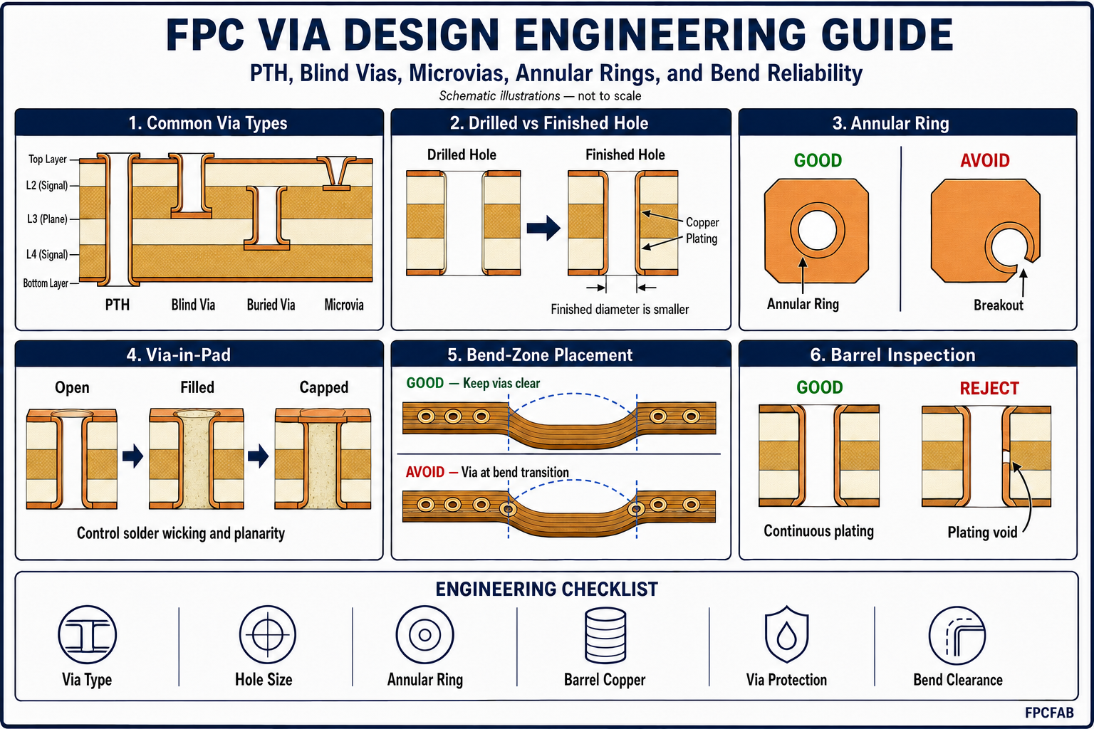
FPC via design must account for more than electrical layer-to-layer connection. Via type, drilled-hole size, finished-hole size, annular ring, copper plating, pad geometry, dielectric thickness, coverlay clearance, and distance from the bend zone all affect fabrication yield and long-term reliability.
A via that is robust in a rigid PCB may become a mechanical weak point in a flexible circuit. The surrounding polyimide moves during handling and bending, while the plated copper barrel and pad create a locally reinforced structure. If the via is placed at a bend transition, near a stiffener edge, or within a repeatedly flexed region, cyclic strain can concentrate at the pad-to-conductor junction or within the plated barrel.
Blind vias, buried vias, and laser-drilled microvias can reduce routing area and support higher interconnect density, but they introduce additional process steps and qualification requirements. Via-in-pad, filled vias, capped vias, and stacked microvias must also be defined by function rather than by abbreviated drawing notes.
This guide explains how engineering and purchasing teams should specify FPC via structures, hole dimensions, annular rings, plating, protection, bend-zone clearance, inspection, and reliability requirements before releasing production data.
1. What an FPC Via Controls
A via provides an electrical connection between conductive layers. In a flexible printed circuit, it also creates a mechanical discontinuity because the copper pad and plated barrel are less flexible than the surrounding dielectric and conductor pattern.
An FPC via may influence:
- Electrical continuity between copper layers
- Current-carrying capability and DC resistance
- Signal return paths and controlled-impedance transitions
- Local stiffness and strain distribution
- Available routing area and conductor density
- Coverlay-opening and pad-exposure requirements
- Assembly planarity when located within a component pad
- Moisture, flux, and contamination entrapment
- Fabrication cost, registration tolerance, and production yield
The design must therefore consider the via as part of the finished mechanical construction, not only as a point in the electrical netlist.
2. Common Via Types Used in FPC Construction
| Via Type | Layer Connection | Typical Manufacturing Method | Engineering Consideration |
|---|---|---|---|
| Plated Through-Hole | Passes through the complete construction | Mechanical drilling followed by copper plating | Established process, but consumes routing area on every layer |
| Blind Via | External layer to one or more internal layers | Mechanical drilling, controlled-depth drilling, or laser processing depending on construction | Requires clear depth, target-layer, and sequential-build definition |
| Buried Via | Connects internal layers without reaching an external surface | Drilling and plating of an internal subassembly before final lamination | Adds lamination and registration complexity |
| Microvia | Normally connects adjacent or selected build-up layers | Laser drilling followed by metallization and copper plating | Requires dielectric, target-pad, fill, stacking, and reliability review |
| Via-in-Pad | Via located inside a component or contact pad | PTH or microvia with specified filling and capping as required | Must control solder wicking, voiding, planarity, and inspection |
A blind via is not automatically a microvia. “Blind” describes which layers are connected, while “microvia” describes a specific small interconnection structure normally produced by laser drilling or another controlled microvia process. Production data should state the actual structure rather than using the two terms interchangeably.
3. Plated Through-Holes in Flexible Circuits
A plated through-hole, commonly abbreviated PTH, extends through the complete flexible-circuit construction. Copper is deposited on the hole wall to connect pads on two or more conductive layers.
PTHs remain common in double-sided and multilayer FPCs because they are well established, inspectable, and compatible with component leads, mounting features, and general layer interconnection. Their mechanical behavior, however, depends on the surrounding stack-up and how the circuit will move in service.
Key PTH design variables
- Drilled-hole diameter
- Finished-hole diameter after copper plating and final finish
- Plated-copper thickness on the hole wall
- Pad diameter and minimum remaining annular ring
- Overall construction thickness and hole aspect ratio
- Hole-to-hole and hole-to-conductor spacing
- Coverlay opening and adhesive-flow allowance
- Distance from stiffener, rigid-section, and bend transitions
The drawing must distinguish drilled-hole size from finished-hole size. A finished hole is smaller because copper plating and surface finish build up on the hole wall. Tolerances should be based on the functional requirement of the finished feature.
4. Blind and Buried Via Structures
Blind and buried vias free routing space on layers that do not require the interconnection. They are useful in dense multilayer FPC and rigid-flex constructions, but they require more detailed process planning than a conventional through-hole.
A blind-via callout should identify:
- Start layer and target layer
- Drilling or laser-processing method
- Hole diameter or permitted feature range
- Target-pad dimensions and registration allowance
- Whether the via is open, filled, capped, or plated over
- Required sequential-lamination structure
- Inspection and qualification method
Buried vias are fabricated within an internal subassembly before final lamination. Their use may increase the number of lamination, drilling, imaging, and plating operations. The cost effect should be reviewed at the stack-up stage rather than after layout completion.
5. Laser-Drilled Microvias
Laser-drilled microvias support high-density interconnect structures where mechanically drilled holes would consume excessive pad and routing area. They are commonly used between adjacent layers or within controlled build-up sequences.
Microvia reliability depends on more than nominal hole diameter. The dielectric thickness, via geometry, target-pad preparation, metallization, copper filling, lamination cycle, material movement, and thermal history all influence performance.
Microvia configurations
- Staggered microvias: Microvias on successive layers are laterally offset, reducing the direct vertical stress path.
- Stacked microvias: Microvias are aligned vertically through multiple build-up layers and normally require filling and specific qualification.
- Microvia-in-pad: A microvia is placed inside a component pad to reduce fan-out area and support fine-pitch packaging.
- Skip microvia: A controlled laser structure connects nonadjacent layers where the process and dielectric construction permit it.
Stacked microvias should not be treated as a simple extension of a single-layer microvia. Each interface adds process and reliability risk. The stack height, fill condition, copper structure, thermal cycling, and supplier capability must be validated for the intended product class.
6. Hole Size, Aspect Ratio, and Fabrication Capability
Hole dimensions should be selected with the complete stack-up and manufacturing process. A small hole in a thin two-layer FPC may be straightforward, while the same nominal hole in a thick multilayer rigid-flex section may require a different drilling and plating strategy.
The aspect ratio is the relationship between the depth of the plated structure and its hole diameter. As the aspect ratio increases, cleaning, activation, metallization, and copper distribution become more difficult. The practical limit depends on the hole type, material system, drilling process, plating equipment, and supplier capability.
For this reason, universal minimum-hole or maximum-aspect-ratio values should not be copied into every FPC drawing. The designer should define the functional requirement and confirm capability with the selected fabricator before design release.
The stack-up review should establish:
- Drilling depth for every hole structure
- Minimum practical drill and finished-hole size
- Required copper thickness in the via barrel
- Expected drill tolerance and positional tolerance
- Available plating distribution across the production panel
- Coupon and inspection requirements
7. Annular Ring and Pad Design
The annular ring is the copper remaining around a drilled or plated hole. Its finished condition reflects pad size, drill size, drill wander, artwork registration, material movement, etching tolerance, and breakout acceptance criteria.
Flexible materials are dimensionally less stable than rigid laminates during lamination, drilling, wet processing, and thermal exposure. Pad geometry must therefore include realistic allowances for the specific FPC construction and panel process.
Teardrops and pad-to-conductor transitions
A teardrop or filleted transition increases copper area where a conductor enters a via pad. This can reduce sensitivity to drill registration and lower stress concentration at the pad-to-trace junction.
Teardrops do not correct an inadequate annular-ring design or an unsuitable bend-zone location. They should be treated as an additional robustness feature, not as permission to reduce other manufacturing allowances.
Good pad-transition practice includes:
- Use smooth fillets rather than abrupt conductor-width changes
- Maintain sufficient copper capture around the hole
- Avoid acute conductor entry angles
- Account for etching and registration tolerances
- Review current density where several conductors converge at one pad
8. Via Placement Relative to the Bend Zone
Via placement is one of the most important mechanical decisions in FPC layout. The via pad, copper barrel, coverlay opening, and any local plating create a stiffness discontinuity. Repeated bending near this discontinuity can produce cracks at the barrel knee, pad interface, or adjacent conductor.
Where practical, vias should be kept outside the active bend zone and away from the line where the circuit exits a stiffener or rigid section.
Recommended bend-zone practice includes:
- Define the active bend region on the mechanical drawing
- Keep PTHs, microvias, exposed pads, and component lands outside that region
- Avoid aligning several vias across the circuit width at one bend line
- Maintain a gradual transition from rigid or stiffened areas into flexible areas
- Do not place a via directly at a stiffener, coverlay, or shielding edge
- Use smooth conductor routing between the via pad and bend region
- Validate unavoidable bend-adjacent vias using representative flex testing
Static installation bends and dynamic-flex applications should not use the same acceptance assumptions. For further guidance, review the FPC Bend Radius Design Guide and the FPC Stiffener Design Guide.
9. Via-in-Pad Design
Via-in-pad places the interconnection inside an SMT, BGA, LGA, wire-bond, contact, or thermal pad. It can reduce routing area and shorten interconnect length, but an open via inside a solderable pad may draw solder into the hole.
Uncontrolled solder wicking can cause insufficient solder volume, component tilt, voiding, nonuniform collapse, or an exposed depression in the assembled pad. Via-in-pad should therefore define the required filling and surface condition.
A via-in-pad specification may require:
- Nonconductive or conductive fill material
- Complete filling or an allowed fill percentage
- Planarization after filling
- Copper capping or plating over the filled via
- Maximum permitted depression, protrusion, or void
- Surface-finish requirements after capping
- Inspection by cross-section, X-ray, or other agreed method
The complete via-in-pad process should be agreed with both the FPC fabricator and assembly provider because bare-board acceptance and solder-joint performance are closely linked.
10. Via Protection, Tenting, Plugging, Filling, and Capping
Terms such as tented, covered, plugged, filled, and capped describe different structures. They should not be used as interchangeable instructions.
| Protection Method | General Description | Typical Reason for Use |
|---|---|---|
| Open Via | Hole remains exposed on one or both sides | Testing, low-cost interconnection, or intentional access |
| Tented Via | Coverlay or other dielectric spans the via opening | Protection from solder, contamination, or handling |
| Covered Via | Via surface is covered by a specified dielectric material | Electrical insulation and environmental protection |
| Plugged Via | Via is partially or fully closed using a specified plugging material | Limit solder flow, contamination, or process ingress |
| Filled Via | Via cavity is filled using a controlled material and process | Via-in-pad, planarity, thermal, or structural requirement |
| Filled and Capped Via | Filled via is planarized and plated over | Planar component pad or high-density interconnect |
IPC-4761 provides terminology and guidance for printed-board via protection. The drawing should state the required protection type, side, material, and acceptance condition. A note that only says “plug all vias” leaves important production details unresolved.
11. Coverlay Openings Around Vias
Coverlay registration and adhesive flow affect the finished via pad. An opening that is too small may reduce accessible pad area or allow adhesive to enter the hole. An opening that is too large may reduce insulation spacing or expose unnecessary conductor area.
The design review should account for:
- Coverlay cutting tolerance
- Coverlay-to-copper registration
- Adhesive squeeze-out during lamination
- Required probe, soldering, or component access
- Minimum dielectric web between adjacent openings
- Whether the via should be exposed, tented, or covered
For additional opening and adhesive-flow guidance, see the FPC Coverlay Design Guide.
12. Copper Plating and Barrel Reliability
The plated barrel must maintain electrical continuity through fabrication, assembly, installation, and service. Reliability depends on hole-wall preparation, desmear or cleaning, metallization, copper distribution, plating thickness, material movement, and the thermal-mechanical loading of the finished circuit.
Potential defects include:
- Voids or discontinuities in the plated barrel
- Thin copper caused by poor plating distribution
- Barrel cracks after thermal cycling or repeated flexing
- Inner-layer separation or inadequate target-pad connection
- Pad lifting caused by excessive mechanical or thermal stress
- Resin, adhesive, or debris remaining on the hole wall
- Cracks at the pad-to-conductor transition
Copper-thickness requirements should refer to the finished plated structure and applicable performance specification. Base copper weight alone does not define the copper condition within the completed hole.
For related copper-construction guidance, review the FPC Copper Foil Guide and the FPC Stack-Up Design Guide.
13. Inspection and Qualification
Inspection should match the via structure and end-use risk. Conventional through-holes, blind vias, filled via-in-pad structures, and stacked microvias do not require identical control plans.
Depending on product class and customer requirements, verification may include:
- Visual inspection of pads, holes, coverlay openings, and filled surfaces
- Finished-hole and pad-diameter measurement
- Microsection evaluation of plating, annular ring, interfaces, and fill condition
- Electrical continuity and isolation testing
- Thermal stress or thermal-cycle testing
- Flex testing using representative bend radius, direction, and cycle count
- X-ray inspection for hidden or filled structures
- Process-coupon testing and lot traceability
Critical medical, automotive, aerospace, industrial, or repeated-flex applications should define qualification requirements before quotation. Test samples must represent the production stack-up, materials, via structure, plating process, and mechanical loading.
14. What to Specify on the Drawing and RFQ
Clear production documentation prevents the fabricator from making assumptions about hole type, dimensions, filling, or acceptance.
Recommended FPC via design information includes:
- Via type and layer connection for every structure
- Drilled-hole size and finished-hole size where applicable
- Pad diameter and minimum annular-ring requirement
- Plated-copper and finished-surface requirements
- Blind, buried, staggered, or stacked-via sequence
- Via-protection type and material
- Via-in-pad filling, planarization, and capping requirement
- Coverlay opening or tenting condition
- Active bend-zone boundaries and minimum keep-out requirements
- Applicable IPC class, standard, and revision
- Required coupons, microsections, thermal testing, and reports
- Component, connector, assembly, and end-use conditions
Relevant standards include IPC-2223E for flexible-board design, IPC-6013E for flexible-board qualification and performance, and IPC-4761 for via-protection guidance.
15. How FPCFAB Supports Via Design and Production
FPCFAB reviews via type, layer connection, hole dimensions, annular rings, copper plating, pad transitions, coverlay openings, via protection, filling, capping, bend-zone clearance, stiffener transitions, and inspection requirements before production.
Our Flexible PCB Manufacturing service supports double-sided, multilayer, and rigid-flex constructions from prototype and NPI builds through production.
Customers may provide completed Gerber or ODB++ data, drill files, stack-up, and fabrication drawings, or request an FPC Design & DFM Review before finalizing the via structure and bend-zone details.
Conclusion
Reliable FPC via design requires more than selecting a nominal hole diameter. Via type, drilling method, finished-hole size, annular ring, plating, pad transition, dielectric thickness, coverlay opening, filling, capping, and mechanical location must be evaluated together.
Plated through-holes remain practical for many double-sided and multilayer FPCs. Blind vias and microvias provide routing-density advantages, but they require a controlled stack-up and qualified fabrication process. Via-in-pad can support fine-pitch assembly when filling, capping, and planarity are properly specified.
Most importantly, vias should be kept outside active bend zones and away from abrupt material transitions wherever possible. When this cannot be achieved, the finished construction should be qualified under representative thermal and mechanical conditions.
For an engineering review or quotation, send your Gerber or ODB++ data, drill files, fabrication drawing, stack-up, via requirements, bend conditions, assembly information, quantities, and application details to FPCFAB.