FPC stack-up design determines far more than the nominal layer count of a flexible printed circuit. The complete construction controls finished thickness, flexibility, copper strain, dimensional stability, impedance, heat resistance, assembly compatibility, manufacturing tolerance, and long-term reliability.
A flexible circuit stack-up cannot be selected by copying a rigid PCB construction and replacing the core material with polyimide. Flexible laminates, copper foil, coverlay, bonding materials, shielding layers, stiffeners, and local adhesive systems behave differently during lamination, assembly, installation, and repeated bending.
Two FPCs with the same layer count can have very different performance. One may be a thin adhesiveless construction designed for dynamic movement, while the other may use adhesive-based laminate, heavier copper, several bonding layers, shielding film, and multiple stiffeners for a static installation.
This guide explains how engineering and purchasing teams should define an FPC stack-up for manufacturability, mechanical reliability, electrical performance, assembly, and quotation.
1. Why FPC Stack-Up Design Is Different From Rigid PCB Design
A rigid PCB is normally designed to remain mechanically stable and substantially flat. Its stack-up is primarily optimized for electrical performance, structural rigidity, thermal behavior, drilling, plating, and assembly.
An FPC must perform as both an electrical interconnect and a mechanical structure. The layers may be bent during installation, folded into a compact enclosure, exposed to vibration, or moved repeatedly during service.
Important differences include:
- Much thinner dielectric and copper constructions
- Greater sensitivity to local thickness changes
- Dimensional movement during lamination and processing
- Mechanical strain in copper and plated features
- Use of coverlay instead of conventional rigid-board solder mask
- Local stiffeners under connectors, components, and contact fingers
- Optional conductive shielding films or copper shields
- Application-specific bend-radius and cycle-life requirements
For industry design guidance applicable to flexible and rigid-flex printed boards, refer to the IPC-2223 sectional design standard.
The FPC stack-up should therefore be defined together with the mechanical drawing, bend conditions, connector requirements, assembly process, operating environment, and expected product life.
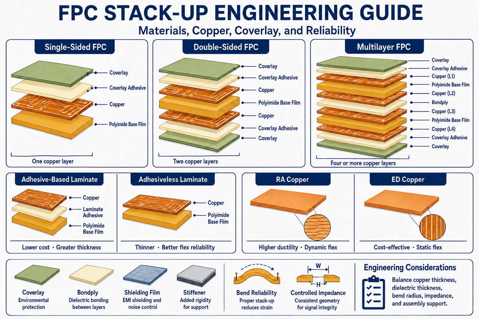
2. Typical Single-Sided FPC Stack-Up
A single-sided flexible circuit contains one conductive copper layer. It is commonly used for simple interconnections, membrane switches, sensor circuits, low-density internal wiring, and applications where plated through-holes are not required.
A typical construction may include:
- Polyimide coverlay film
- Coverlay adhesive
- Copper conductor layer
- Adhesive or direct copper-to-polyimide interface
- Polyimide base film
- Optional backside coverlay, adhesive, or local reinforcement
Single-sided FPCs can provide excellent flexibility because the construction is thin and contains only one copper layer. However, flexibility still depends on copper thickness, foil type, coverlay, adhesive thickness, local stiffeners, and conductor routing.
When the circuit requires exposed contacts, the coverlay drawing should clearly define the opening dimensions, surface finish, contact length, and any local stiffener used to control insertion thickness.
3. Typical Double-Sided FPC Stack-Up
A double-sided FPC contains copper on both sides of the flexible dielectric. The two copper layers may be interconnected through plated through-holes or vias.
A typical double-sided construction may include:
- Top coverlay film and adhesive
- Top copper layer
- Polyimide dielectric with or without laminate adhesive
- Bottom copper layer
- Bottom coverlay film and adhesive
- Plated through-holes where interconnection is required
A balanced double-sided construction can provide better mechanical symmetry than an unbalanced stack-up. However, copper distribution, plating buildup, coverlay openings, shielding, and stiffeners can still create local imbalance.
Plated holes and annular rings increase local stiffness and should normally remain outside active dynamic bend zones. If the circuit bends close to a via field, the transition distance and local copper design require careful review.
4. Multilayer FPC Stack-Up
Multilayer flexible circuits contain three or more conductive layers. They are used when the product requires higher routing density, shielding, power distribution, controlled impedance, or complex interconnection within limited space.
A multilayer FPC may include:
- Outer coverlay layers
- Multiple copper conductor layers
- Polyimide dielectric layers
- Bondply or bonding-film layers
- Plated through-holes, blind vias, or other approved interconnections
- Reference planes, shielding layers, or crosshatched copper
- Local stiffeners and assembly reinforcement
Each additional layer increases finished thickness and manufacturing complexity. Multilayer constructions also require tighter control of registration, lamination movement, drilling, plating, dielectric thickness, coverlay alignment, and final outline accuracy.
For dynamic-flex applications, the copper layers should be positioned as close as practical to the neutral axis, and the construction should remain thin and mechanically balanced. A multilayer circuit should not be assumed suitable for continuous movement solely because it uses flexible dielectric materials.
Detailed mechanical considerations are explained in our FPC Bend Radius Design Guide.
5. Adhesive-Based and Adhesiveless Flexible Laminates
The base laminate is one of the most important FPC stack-up decisions. Flexible copper-clad laminate is generally classified as adhesive-based or adhesiveless.
Adhesive-Based Laminate
Adhesive-based laminate contains an adhesive layer between the copper foil and the polyimide base film. It is widely used in many commercial and static-flex applications.
Potential advantages include:
- Broad material availability
- Established processing methods
- Suitability for many standard FPC applications
- Competitive material cost
The adhesive increases total thickness and may influence dimensional stability, thermal behavior, moisture response, and flex performance. Its suitability should be evaluated against the assembly temperature and product environment.
Adhesiveless Laminate
Adhesiveless laminate does not use a separate adhesive layer between the base copper and polyimide dielectric. It is commonly selected for thin, high-density, controlled-impedance, and higher-reliability constructions.
Potential advantages include:
- Reduced finished thickness
- Improved dimensional control in suitable constructions
- Reduced dielectric complexity
- Good compatibility with fine features and dynamic-flex designs
- Improved thermal capability for demanding assembly processes
Adhesiveless material may cost more than standard adhesive-based laminate and can require more controlled material procurement. It should be selected because the application benefits from its properties, not simply because it is described as a higher-grade material.
6. RA Copper vs ED Copper
Copper foil type directly influences bending behavior, conductor fatigue, etching, plating, and material cost.
Rolled Annealed Copper
Rolled annealed copper is generally preferred for dynamic-flex and high-cycle applications because its elongated grain structure provides improved resistance to repeated bending.
RA copper is also commonly considered when the circuit must be formed tightly during installation or exposed to repeated mechanical movement.
However, RA copper alone does not guarantee flex reliability. Copper thickness, conductor direction, plated buildup, bend radius, total construction thickness, stiffener transitions, and local strain remain important.
Electrodeposited Copper
Electrodeposited copper is widely used in static-flex, installation-flex, and cost-sensitive applications. Different ED copper grades can provide different mechanical performance, so the exact material should be reviewed when cycle life is important.
The decision between RA and ED copper should be based on:
- Static or dynamic flexing condition
- Required cycle life
- Bend radius
- Copper thickness
- Electrical current requirement
- Fine-line manufacturing requirement
- Material availability and cost
7. Base Copper and Finished Copper Thickness
The starting copper foil thickness is not always the same as the final copper thickness shown on the finished product. Plating can add copper to through-holes, vias, annular rings, and exposed conductor surfaces depending on the manufacturing process.
The stack-up drawing should distinguish between:
- Base copper foil thickness
- Plated copper thickness
- Finished conductor thickness
- Finished copper requirement in plated-hole areas
Thicker copper improves current-carrying capability but increases stiffness, etching difficulty, and bending strain. When space permits, increasing conductor width may be mechanically preferable to increasing copper thickness in an active bend region.
Heavy copper combined with narrow spacing can also increase etching and registration risk. Electrical, mechanical, and manufacturing requirements should therefore be reviewed together.
8. Coverlay, Covercoat, Bondply, and Adhesive Systems
Coverlay
Coverlay is the primary protective insulation used over flexible circuit conductors. A conventional coverlay normally consists of polyimide film and an adhesive layer.
The coverlay drawing should define:
- Film thickness
- Adhesive thickness
- Opening dimensions
- Registration tolerance
- Clearance from pads and contact fingers
- Termination near bend and stiffener transitions
Coverlay adhesive must flow sufficiently during lamination to bond and encapsulate the conductor pattern. Excessive adhesive flow can contaminate pads or reduce opening dimensions, while insufficient flow can create voids or poor conductor-edge coverage.
Photoimageable Covercoat
Photoimageable covercoat may be used when the design requires fine-pitch openings or complex pad geometry that is difficult to achieve with mechanically or laser-processed film coverlay.
Its mechanical flexibility, thickness, adhesion, assembly compatibility, and application environment should be reviewed before it is selected for an active flex region.
Bondply and Bonding Film
Bondply or bonding film is used to bond internal layers in multilayer flexible circuits and rigid-flex constructions. Its thickness and cured behavior influence the final dielectric spacing, overall thickness, dimensional movement, and impedance.
The manufacturer should review resin or adhesive flow around copper features, drilled holes, transition areas, and local openings before confirming the multilayer construction.
9. Finished Thickness and Mechanical Reliability
The finished FPC thickness should include the complete material construction in each functional region. A single nominal value may not accurately describe areas containing stiffeners, shielding, PSA, exposed contacts, components, or local reinforcement.
Important thickness values may include:
- Finished thickness in the active flex region
- Finished thickness in connector areas
- ZIF insertion thickness
- Thickness under components
- Thickness at shielding overlaps
- Thickness at stiffener transitions
Increasing total thickness generally increases bending strain. For dynamic-flex applications, unnecessary adhesive, coverlay, shielding, and reinforcement should be kept out of the active bend zone.
A thin stack-up is not automatically reliable. The copper routing, layer balance, material transitions, bend radius, and assembly handling must also be controlled.
10. Shielding Film, Copper Shield, and Reference Planes
Many FPCs require EMI shielding or an electrical reference plane. Shielding can be provided by conductive film, copper foil, solid copper planes, crosshatched copper, or a combination of methods.
The shielding design affects:
- Finished thickness
- Bending stiffness
- Grounding and termination
- Controlled impedance
- Assembly temperature exposure
- Adhesion and delamination risk
- Flex-cycle capability
Conductive shielding film is thin and can provide effective coverage, but it still adds stiffness and requires defined grounding points. Shielding-film edges and grounding areas should not create abrupt material transitions inside active bend zones.
A solid copper shield can provide strong electrical shielding but may make the circuit too stiff for repeated flexing. Crosshatched copper can improve flexibility, but the hatch geometry, conductor direction, impedance, current return path, and manufacturing capability must be evaluated.
11. Stiffeners, PSA, and Local Reinforcement
Stiffeners are used where the FPC requires local mechanical support. Common stiffener materials include polyimide, FR4, stainless steel, and aluminum.
Typical stiffener locations include:
- ZIF contact fingers
- Board-to-board connector areas
- SMT component regions
- Mounting holes
- Soldered wire or terminal areas
- Mechanical attachment points
The stiffener drawing should define material, thickness, outline, adhesive, alignment tolerance, and relationship to the finished FPC outline.
Stiffener edges should remain outside active bend zones. Rounded corners and adequate transition distance help reduce local stress concentration.
Pressure-sensitive adhesive may be used to mount the FPC into the final product. PSA type, thickness, release liner, application area, operating temperature, and bonding surface should be defined. PSA should not unintentionally restrict an active flex region.
12. Controlled-Impedance FPC Stack-Up
Controlled-impedance FPCs require coordinated control of conductor geometry and dielectric construction.
The impedance review should include:
- Single-ended or differential impedance target
- Trace width and spacing
- Base and finished copper thickness
- Dielectric thickness
- Material dielectric properties
- Coverlay film and adhesive
- Reference-plane structure
- Shielding film or copper shield
- Crosshatch geometry where used
- Test-coupon and test-report requirements
Coverlay can change the effective dielectric environment around the conductor and should be included in the impedance model. The approved stack-up should clearly identify the reference layer and dielectric spacing.
Impedance should not be controlled by copying a trace width from a rigid PCB or another unrelated FPC stack-up. The actual materials and finished construction must be modeled and verified.
13. FPC Stack-Up Requirements for FPCA
When components are assembled onto the flexible circuit, the stack-up must support both fabrication and assembly.
FPCA-related considerations include:
- Local flatness under components
- Stiffener thickness and position
- Reflow-temperature compatibility
- Moisture handling and prebaking where required
- Assembly carrier or fixture design
- Pad, coverlay, and solder-paste geometry
- Component mass and mechanical loading
- Connector insertion and retention forces
- Inspection and functional testing
Heavy components, connectors, solder joints, and stiffener edges should not be placed in active bend regions unless the product uses a validated reinforcement strategy.
For integrated fabrication and assembly support, see our Flexible PCB Assembly / FPCA service.
14. Manufacturing Tolerances and DFM Review
An FPC stack-up drawing should state realistic nominal values and tolerances. Flexible materials move during lamination, imaging, drilling, coverlay processing, stiffener bonding, and final profiling.
Important manufacturing controls include:
- Finished overall thickness and tolerance
- Dielectric thickness and tolerance
- Base and finished copper thickness
- Coverlay opening and registration tolerance
- Stiffener alignment and outline tolerance
- ZIF insertion thickness
- Impedance tolerance
- Final outline and hole-location tolerance
Overly tight general tolerances can increase manufacturing cost and reduce yield without improving product function. Critical connector, mechanical, and impedance dimensions should be identified separately from non-critical dimensions.
FPCFAB provides FPC Design & DFM Review for materials, stack-up, coverlay, bend areas, stiffeners, impedance, connector regions, tolerances, and assembly risks.
15. Information Required for FPC Stack-Up Quotation
Provide the following information whenever available:
- Layer count
- Proposed stack-up
- Base and finished copper thickness
- RA or ED copper requirement
- Adhesive-based or adhesiveless laminate requirement
- Coverlay film and adhesive thickness
- Finished overall thickness
- Shielding construction
- Stiffener material, thickness, and location
- Pressure-sensitive adhesive requirement
- Controlled-impedance values
- Bend radius and cycle-life requirement
- Assembly and operating temperature
- Required inspection and quality documentation
When the stack-up is not yet finalized, provide the electrical, mechanical, assembly, and application requirements. The manufacturer can propose a preliminary construction for review.
For a broader RFQ checklist, read How to Prepare an FPC RFQ.
FPC Stack-Up Review Checklist
| Review Area | Questions to Confirm |
|---|---|
| Application | Is the circuit static flex, installation flex, limited-cycle flex, or dynamic flex? |
| Layer count | Is the minimum practical number of copper layers being used? |
| Laminate | Is adhesive-based or adhesiveless material appropriate for thickness, temperature, density, and flex life? |
| Copper foil | Are RA or ED copper, base thickness, finished thickness, and plating suitable? |
| Coverlay | Are film, adhesive, openings, registration, and bend-zone transitions defined? |
| Thickness | Are active-flex, connector, stiffened, shielded, and assembly-region thicknesses controlled? |
| Shielding | Are shielding material, grounding, stiffness, impedance, and transition areas reviewed? |
| Stiffeners | Are material, thickness, adhesive, outline, tolerance, and edge location defined? |
| Impedance | Are dielectric thickness, copper, coverlay, reference planes, shielding, and testing included? |
| Assembly | Is the stack-up compatible with component support, fixtures, reflow, handling, and testing? |
| DFM | Are material availability, manufacturing tolerance, registration, yield, and cost reviewed? |
How FPC Stack-Up Affects Cost
FPC stack-up directly affects material cost, tooling, lamination, drilling, plating, coverlay processing, stiffener bonding, shielding, impedance testing, yield, and lead time.
Cost can increase when the design requires:
- Additional copper and dielectric layers
- Adhesiveless or special high-temperature materials
- RA copper or uncommon copper thicknesses
- Tight finished-thickness tolerances
- Fine-pitch coverlay openings
- Multiple or metal stiffeners
- Conductive shielding films
- Controlled impedance and test coupons
- Special traceability or inspection reports
A lower-cost stack-up should not be achieved by removing required materials, weakening mechanical support, or changing controlled materials without engineering approval.
For detailed pricing considerations, read What Affects FPC Cost?.
How FPCFAB Supports FPC Stack-Up Development
FPCFAB reviews layer count, laminate type, copper foil, copper thickness, coverlay, bondply, finished thickness, shielding, stiffeners, PSA, controlled impedance, bend requirements, manufacturing tolerances, and assembly conditions before production.
Our Flexible PCB Manufacturing service supports single-sided, double-sided, and multilayer flexible circuit projects from prototype and NPI through pilot-run and production stages.
Customers may provide a completed stack-up or submit preliminary electrical and mechanical requirements for engineering review.
Conclusion
FPC stack-up design should balance electrical performance, mechanical flexibility, finished thickness, copper reliability, assembly compatibility, manufacturing tolerance, and cost.
The correct construction depends on the application. Single-sided, double-sided, multilayer, static-flex, dynamic-flex, shielded, controlled-impedance, and assembled FPCs each require different material and structural decisions.
Material names alone do not define a reliable stack-up. Copper foil, adhesive, coverlay, bonding layers, shielding, stiffeners, local thickness changes, bend conditions, and production capability must be reviewed as one complete system.
Send your Gerber files, fabrication drawing, proposed stack-up, bend requirements, impedance values, stiffener information, quantities, and assembly data to FPCFAB for engineering review and quotation support.